Pages

Subscribe:

Ads 468x60px

Showing posts with label Research and Development. Show all posts

Friday, February 3, 2012

Mitsubishi Electric Announces New Ultra-High-Speed Elevator Technologies

Engineerblogger
Feb 3, 2012

Shanghai Tower will represent China's dynamic 'future

Mitsubishi Electric Corporation announced today its new suite of technologies that enable ultra-high-speed elevators to travel faster than 1,000 meters per minute, or 60 kph, with enhanced efficiency, comfort and safety. The technologies will be incorporated in the world's fastest elevators, including those developed by Mitsubishi Electric for the 632-meter Shanghai Tower under construction in Shanghai, China.

In response to the increasing height of high-rise buildings amid continuing urban population growth, the role of elevators is gaining even greater importance. In response, Mitsubishi Electric is developing advanced solutions incorporating technologies and equipment for enhanced drive and controllability, safety, super high-rise cable mechanics and passenger comfort. The company's new suite of ultra-high-speed elevator technologies includes the following advancements:

1.  Drive and Controllability
  • The traction motor incorporates a permanent magnetic motor for energy-efficient, low-noise, low-vibration operation.
  • A single motor has two grouped three-phase winding coils and parallel drive systems controlled by separate control panels. Each motor has a built-in converter to regenerate electricity, lowering power consumption by more than 30 percent.
  • Brakes composed of two units with a hydraulic driven clamp-type disk brake achieve stable braking.
 
2.  Safety

  • Safety gears, which activate the brakes by grasping the guide rails in emergencies if cables become transected, comprise two stages to manage increased kinetic energy due to ultra-high speeds.
  • Fine ceramic is used for the safety gear shoe to realize high resistance to heat, abrasion and shock. Braking is extra-stable even if high frictional heat is generated when the safety gear is activated.
  • The hydraulic oil buffer (shock absorber) at the bottom of the elevator shaft has an advanced plunger comprising three stages for exceptional shock absorption within a shortened frame.
  • Newly developed governor monitors elevator speed stably even with heavy loads placed by ropes traveling at high speeds over long distances.

3.  Super high-rise cable mechanics

  • A steel core with a wider diameter provides high intensity, allowing traveling cables to be lightened by using lightweight sheath material and operated by a highly efficient electric power carrier system.
  • Mitsubishi Electric's new "sfleX-rope" comprising bundles of high-intensity steel wire strands, each covered with plastic, offers higher intensity than conventional rope for safe operation despite the greater weight of longer ropes. Each wire has a higher density and wider cross-sectional area than conventional rope, which helps to reduce rope stretching caused when passengers step onto the elevator.


4.  Ride comfort
  •   A new active roller guide, which reduces vibration from the guide rails and wind, enhances passenger comfort even at ultra-high speeds.
  •   The inside of the car is extra-quiet thanks to a streamlined aerodynamic car cover and a high sound insulation cage.
  • Air pressure control helps to minimize rapid changes in atmospheric pressure for reduced ear discomfort.

Just like cars, going that fast also leads to the question of safety – rest assured that Mitsubishi will deliver enhanced efficiency, comfort and safety as thousands of people traverse through these elevators each day. Fine ceramic is the material of choice for the safety gear shoe as it has a high resistance to heat, abrasion and shock. Never mind if high frictional heat is generated, braking remains extremely stable.

Source: Mitsubishi Electric Corporation

Biosolar Breakthrough Promises Cheap, Easy Green Electricity

Engineerblogger
Feb 3, 2012


Barry D. Bruce

Barry D. Bruce, professor of biochemistry, cellular and molecular biology, at the University of Tennessee, Knoxville, is turning the term “power plant” on its head. The biochemist and a team of researchers have developed a system that taps into photosynthetic processes to produce efficient and inexpensive energy.

Bruce collaborated with researchers from the Massachusetts Institute of Technology and Ecole Polytechnique Federale in Switzerland to develop a process that improves the efficiency of generating electric power using molecular structures extracted from plants. The biosolar breakthrough has the potential to make “green” electricity dramatically cheaper and easier.

“This system is a preferred method of sustainable energy because it is clean and it is potentially very efficient,” said Bruce, who was named one of “Ten Revolutionaries that May Change the World” by Forbes magazine in 2007 for his early work, which first demonstated biosolar electricity generation. “As opposed to conventional photovoltaic solar power systems, we are using renewable biological materials rather than toxic chemicals to generate energy. Likewise, our system will require less time, land, water and input of fossil fuels to produce energy than most biofuels.”

Their findings are in the current issue of Nature: Scientific Reports.

To produce the energy, the scientists harnessed the power of a key component of photosynthesis known as photosystem-I (PSI) from blue-green algae. This complex was then bioengineered to specifically interact with a semi-conductor so that, when illuminated, the process of photosynthesis produced electricity. Because of the engineered properties, the system self-assembles and is much easier to re-create than his earlier work. In fact, the approach is simple enough that it can be replicated in most labs—allowing others around the world to work toward further optimization.

“Because the system is so cheap and simple, my hope is that this system will develop with additional improvements to lead to a green, sustainable energy source,” said Bruce, noting that today’s fossil fuels were once, millions of years ago, energy-rich plant matter whose growth also was supported by the sun via the process of photosynthesis.

This green solar cell is a marriage of non-biological and biological materials. It consists of small tubes made of zinc oxide—this is the non-biological material. These tiny tubes are bioengineered to attract PSI particles and quickly become coated with them—that’s the biological part. Done correctly, the two materials intimately intermingle on the metal oxide interface, which when illuminated by sunlight, excites PSI to produce an electron which “jumps” into the zinc oxide semiconductor, producing an electric current.

The mechanism is orders of magnitude more efficient than Bruce’s earlier work for producing bio-electricity thanks to the interfacing of PSI with the large surface provided by the nanostructured conductive zinc oxide; however it still needs to improve manifold to become useful. Still, the researchers are optimistic and expect rapid progress.

Bruce’s ability to extract the photosynthetic complexes from algae was key to the new biosolar process. His lab at UT isolated and bioengineered usable quantities of the PSI for the research.


Algae could be the next power source. Credit: University of Tennessee, Knoxville

Andreas Mershin, the lead author of the paper and a research scientist at MIT, conceptualized and created the nanoscale wires and platform. He credits his design to observing the way needles on pine trees are placed to maximize exposure to sunlight.

Mohammad Khaja Nazeeruddin in the lab of Michael Graetzel, a professor at the Ecole Polytechnique Federale in Lausanne, Switzerland, did the complex testing needed to determine that the new mechanism actually performed as expected. Graetzel is a pioneer in energy and electron transfer reactions and their application in solar energy conversion.

Michael Vaughn, once an undergraduate in Bruce’s lab and now a National Science Foundation (NSF) predoctoral fellow at Arizona State University, also collaborated on the paper.

“This is a real scientific breakthrough that could become a significant part of our renewable energy strategy in the future,” said Lee Riedinger, interim vice chancellor for research. “This success shows that the major energy challenges facing us require clever interdisciplinary solutions, which is what we are trying to achieve in our energy science and engineering PhD program at the Bredesen Center for Interdisciplinary Research and Graduate Education of which Dr. Bruce is one of the leading faculty.”

The Bredesen Center is a joint UT/Oak Ridge National Laboratory academic unit. Bruce is also a co-principal investigator and scientific thrust leader in TN: SCORE, the Tennessee Solar Conversion and Storage Using Outreach, Research and Education. The $20 million project is funded by the NSF and focuses on promoting research and education on solar energy problems across Tennessee. Additionally, he co-founded and is associate director of UT’s Sustainable Energy Education.

Bruce’s work is funded by the Emerging Frontiers Program at the National Science Foundation.


Source: University of Tennessee, Knoxville

Related Information:

Graphene electronics moves into a third dimension

Engineerblogger
Feb 3, 2012


Graphene nanofabric. SEM micrograph of a strongly crumpled graphene sheet on a Si wafer. Note that it looks just like silk thrown over a surface. Lateral size of the image is 20 microns. Si wafer is at the bottom-right corner. Credit: University of Manchester

In a paper published this week in Science, a Manchester team lead by Nobel laureates Professor Andre Geim and Professor Konstantin Novoselov has literally opened a third dimension in graphene research. Their research shows a transistor that may prove the missing link for graphene to become the next silicon.

Graphene – one atomic plane of carbon – is a remarkable material with endless unique properties, from electronic to chemical and from optical to mechanical.

One of many potential applications of graphene is its use as the basic material for computer chips instead of silicon. This potential has alerted the attention of major chip manufactures, including IBM, Samsung, Texas Instruments and Intel. Individual transistors with very high frequencies (up to 300 GHz) have already been demonstrated by several groups worldwide.

Unfortunately, those transistors cannot be packed densely in a computer chip because they leak too much current, even in the most insulating state of graphene. This electric current would cause chips to melt within a fraction of a second.

This problem has been around since 2004 when the Manchester researchers reported their Nobel-winning graphene findings and, despite a huge worldwide effort to solve it since then, no real solution has so far been offered.

The University of Manchester scientists now suggest using graphene not laterally (in plane) – as all the previous studies did – but in the vertical direction. They used graphene as an electrode from which electrons tunnelled through a dielectric into another metal. This is called a tunnelling diode.

Then they exploited a truly unique feature of graphene – that an external voltage can strongly change the energy of tunnelling electrons. As a result they got a new type of a device – vertical field-effect tunnelling transistor in which graphene is a critical ingredient.

Dr Leonid Ponomarenko, who spearheaded the experimental effort, said: “We have proved a conceptually new approach to graphene electronics. Our transistors already work pretty well. I believe they can be improved much further, scaled down to nanometre sizes and work at sub-THz frequencies.”

“It is a new vista for graphene research and chances for graphene-based electronics never looked better than they are now”, adds Professor Novoselov.

Graphene alone would not be enough to make the breakthrough. Fortunately, there are many other materials, which are only one atom or one molecule thick, and they were used for help.

The Manchester team made the transistors by combining graphene together with atomic planes of boron nitride and molybdenum disulfide. The transistors were assembled layer by layer in a desired sequence, like a layer cake but on an atomic scale.

Such layer-cake superstructures do not exist in nature. It is an entirely new concept introduced in the report by the Manchester researchers. The atomic-scale assembly offers many new degrees of functionality, without some of which the tunnelling transistor would be impossible.

“The demonstrated transistor is important but the concept of atomic layer assembly is probably even more important,” explains Professor Geim.

Professor Novoselov added: “Tunnelling transistor is just one example of the inexhaustible collection of layered structures and novel devices which can now be created by such assembly.

“It really offers endless opportunities both for fundamental physics and for applications. Other possible examples include light emission diodes, photovoltaic devices, and so on.”

Source: University of Manchester

Additional Information:

Tuesday, January 31, 2012

Device Could Drive Down Solar's Cost

Technology Review
Jan 31, 2012
 
Power play: Inverters mounted to the bottom of each panel provide grid-ready power at a test site in Sunnyvale, California. Credit: ArrayPower

As solar panel manufacturers try to harvest more of the sun's energy for less, they face increasingly diminishing returns. At roughly $1 per watt, the cost of solar modules now represents less than a third of the total cost of commercial solar installations. To cut the total cost of solar power—currently $3.00 to $3.50 per watt—bigger gains will have to come from improvements in the power electronics, wiring, and mounting systems required for solar installations.

ArrayPower, a startup based in Sunnyvale, California, has developed a new type of solar inverter—the device that converts direct current (DC) power produced by solar panels to grid-ready, alternating current (AC) electricity—that it claims could significantly reduce the cost of solar power. The company says its "sequenced inverter" will reduce the cost of commercial solar by 35 cents per watt, or more than 10 percent, by lowering capital costs, simplifying installation, and increasing output.

Large-scale solar installations currently use either a single "central" inverter or a number of "string" inverters to convert power from groups of panels strung together in series. Both approaches, however, suffer from low efficiencies because of the way the panels are connected. In either scenario, if one panel is damaged or shaded from the sun, the system's entire output is diminished to the level of its lowest-producing panel.

ArrayPower seeks to maximize power output through a new type of inverter mounted to each panel. The device is similar to microinverters now used in residential solar installations. By converting DC to AC power at each module, microinverters maximize the power output of each module, thereby increasing system output by roughly 3 percent to 10 percent.

Microinverters are typically more expensive because they require sophisticated electronics to filter and smooth the alternating current coming out of each inverter. A major cost is an electrolytic capacitor, essentially a chemical battery that stores energy for short bursts, allowing the inverter to send out pulses of electricity that create an alternating current. Further, microinverters typically only yield single-phase AC electricity, an electric current that is suited for residential use but not commercial or utility use.
To read more click here...

Monday, January 30, 2012

Keeping high-performance electronics cool

Engineerblogger
Jan 30, 2012


The development of sophisticated electronics using high-performance computer chips that generate much more heat than conventional chips is challenging scientists to come up with a new type of compact cooling system to keep temperatures under control.

For the past few years, a collaborative team of engineers and other scientists from academia and industry has been investigating an advanced cooling system for electric and hybrid cars as well as computers and telecommunications systems, particularly for military use in radar, lasers, and electronics in aircraft.

The technology, which is capable of handling roughly 10 times the heat generated by conventional chips, is a device, called a vapor chamber, using tiny copper spheres and carbon nanotubes to passively wick a coolant toward hot electronics, according to Suresh V. Garimella, the R. Eugene and Susie E. Goodson Distinguished Professor in the School of Mechanical Engineering at Purdue University, West Lafayette, IN.

The current thermal solution it would replace is typically a solid heat spreader using solid aluminum and copper to conduct heat, an approach inadequate for removing large amounts of heat in powerful electronics components while maintaining low operating temperatures.

A Passive System

The vapor chamber comes in the same form factor as a solid heat spreader, says Dr. Garimella, but "The working fluid contained inside continuously undergoes [evaporation] at the heat source to more efficiently remove heat than is possible by devices that rely on conduction alone."

An advantage of vapor chambers compared to other high-performance cooling technology alternatives is that a vapor chamber is a completely passive system. According to Dr. Garimella, "It can…operate continuously without any additional pumps or valves. Such passive systems are associated with high reliability. Active cooling options which allow for high heat dissipation, such as forced liquid cooling, require an external fluid flow system including a separate pump and condenser, adding to the solution cost and size."

Much of the work is being conducted at the Industry/University Cooperative Research Center's Cooling Technologies Research Center, established by Dr. Garimella at Purdue.

Integrating Nanostructures

After publishing its findings last year about the effects of conventional sintered powder copper structures on the performance of a vapor-chamber cooling technology, the team is preparing to report on the feasibility of integrating nanostructures, specifically carbon nanotubes, into the devices to further improve performance. These results and proposed techniques for integrating carbon nanotubes into vapor chambers are expected to be published in the near future, says Dr. Garimella.

"The next step is to experimentally investigate the performance enhancement provided by integration of carbon nanotubes into vapor chambers," he says. "Another critical step in converting performance enhancements observed in the lab to actual devices is to develop engineering models and methods that allow accurate prediction of device performance for specific applications."

When the program, which is being funded by the U.S. Department of Defense's Defense Advanced Research Projects Agency, is completed at the end of this year, the hope is that there will be transition to actual applications, especially for the Department of Defense, where there is significant need, says Dr. Garimella.

Source: American Society of Mechanical Engineers (ASME)

Tuesday, January 24, 2012

Cooling semiconductor by laser light

Engineerblogger
Jan 24, 2012


Koji Usami is working in the Quantop laboratories at the Niels Bohr Institute. Photo: Ola J. Joensen

Researchers at the Niels Bohr Institute have combined two worlds – quantum physics and nano physics, and this has led to the discovery of a new method for laser cooling semiconductor membranes. Semiconductors are vital components in solar cells, LEDs and many other electronics, and the efficient cooling of components is important for future quantum computers and ultrasensitive sensors. The new cooling method works quite paradoxically by heating the material! Using lasers, researchers cooled membrane fluctuations to minus 269 degrees C. The results are published in the scientific journal, Nature Physics.

“In experiments, we have succeeded in achieving a new and efficient cooling of a solid material by using lasers. We have produced a semiconductor membrane with a thickness of 160 nanometers and an unprecedented surface area of 1 by 1 millimeter. In the experiments, we let the membrane interact with the laser light in such a way that its mechanical movements affected the light that hit it. We carefully examined the physics and discovered that a certain oscillation mode of the membrane cooled from room temperature down to minus 269 degrees C, which was a result of the complex and fascinating interplay between the movement of the membrane, the properties of the semiconductor and the optical resonances,” explains Koji Usami, associate professor at Quantop at the Niels Bohr Institute.

From gas to solid

Laser cooling of atoms has been practiced for several years in experiments in the quantum optical laboratories of the Quantop research group at the Niels Bohr Institute. Here researchers have cooled gas clouds of cesium atoms down to near absolute zero, minus 273 degrees C, using focused lasers and have created entanglement between two atomic systems. The atomic spin becomes entangled and the two gas clouds have a kind of link, which is due to quantum mechanics. Using quantum optical techniques, they have measured the quantum fluctuations of the atomic spin.

“For some time we have wanted to examine how far you can extend the limits of quantum mechanics – does it also apply to macroscopic materials? It would mean entirely new possibilities for what is called optomechanics, which is the interaction between optical radiation, i.e. light, and a mechanical motion,” explains Professor Eugene Polzik, head of the Center of Excellence Quantop at the Niels Bohr Institute at the University of Copenhagen.

But they had to find the right material to work with.

The experiments are carried out in the Quantop laboratories at the Niels Bohr Institute. The laser light that hits the semiconducting nanomembrane is controlled with a forest of mirrors. Photo: Ola J. Joensen

Lucky coincidence

In 2009, Peter Lodahl (who is today a professor and head of the Quantum Photonic research group at the Niels Bohr Institute) gave a lecture at the Niels Bohr Institute, where he showed a special photonic crystal membrane that was made of the semiconducting material gallium arsenide (GaAs). Eugene Polzik immediately thought that this nanomembrane had many advantageous electronic and optical properties and he suggested to Peter Lodahl’s group that they use this kind of membrane for experiments with optomechanics. But this required quite specific dimensions and after a year of trying they managed to make a suitable one.

“We managed to produce a nanomembrane that is only 160 nanometers thick and with an area of more than 1 square millimetre. The size is enormous, which no one thought it was possible to produce,” explains Assistant Professor Søren Stobbe, who also works at the Niels Bohr Institute.

Koji Usami shows the holder with the semiconductor nanomembrane. The holder measures about one by cm, while the nanomembrane itself has a surface area of 1 by 1 millimeter and a thickness of 160 nanometers. Photo: Ola J. Joensen

Basis for new research

Now a foundation had been created for being able to reconcile quantum mechanics with macroscopic materials to explore the optomechanical effects.

Koji Usami explains that in the experiment they shine the laser light onto the nanomembrane in a vacuum chamber. When the laser light hits the semiconductor membrane, some of the light is reflected and the light is reflected back again via a mirror in the experiment so that the light flies back and forth in this space and forms an optical resonator. Some of the light is absorbed by the membrane and releases free electrons. The electrons decay and thereby heat the membrane and this gives a thermal expansion. In this way the distance between the membrane and the mirror is constantly changed in the form of a fluctuation.

"Changing the distance between the membrane and the mirror leads to a complex and fascinating interplay between the movement of the membrane, the properties of the semiconductor and the optical resonances and you can control the system so as to cool the temperature of the membrane fluctuations. This is a new optomechanical mechanism, which is central to the new discovery. The paradox is that even though the membrane as a whole is getting a little bit warmer, the membrane is cooled at a certain oscillation and the cooling can be controlled with laser light. So it is cooling by warming! We managed to cool the membrane fluctuations to minus 269 degrees C", Koji Usami explains.

“The potential of optomechanics could, for example, pave the way for cooling components in quantum computers. Efficient cooling of mechanical fluctuations of semiconducting nanomembranes by means of light could also lead to the development of new sensors for electric current and mechanical forces. Such cooling in some cases could replace expensive cryogenic cooling, which is used today and could result in extremely sensitive sensors that are only limited by quantum fluctuations,” says Professor Eugene Polzik.

Source: University of Copenhagen

Water sees right through graphene: graphene enhances many materials, but leaves them wettable

Engineerblogger
Jan 24, 2012
Dropsof water on a piece of silicon and on silicon covered by a layer of grapheneshow a minimal change in the contact angle between the water and the basematerial. Researchers at Rice University and Rensselaer Polytechnic Institutedetermined that when applied to most metals and silicon, a single layer ofgraphene is transparent to water. (Credit: Rahul Rao/Rensselaer Polytechnic Institute)

Graphene is largely transparent to the eye and, as it turns out, largely transparent to water.

A new study by scientists at Rice University and Rensselaer Polytechnic Institute (RPI) has determined that gold, copper and silicon get just as wet when clad by a single continuous layer of graphene as they would without.

The research, reported this week in the online edition of Nature Materials, is significant for scientists learning to fine-tune surface coatings for a variety of applications.

"The extreme thinness of graphene makes it a totally non-invasive coating," said Pulickel Ajayan, Rice's Benjamin M. and Mary Greenwood Anderson Professor in Mechanical Engineering and Materials Science and of chemistry. "A drop of water sitting on a surface 'sees through' the graphene layers and conforms to the wetting forces dictated by the surface beneath. It's quite an interesting phenomenon unseen in any other coatings and once again proves that graphene is really unique in many different ways." Ajayan is co-principal investigator of the study with Nikhil Koratkar, a professor of mechanical, aerospace and nuclear engineering at RPI.

A typical surface of graphite, the form of carbon most commonly known as pencil lead, should be hydrophobic, Ajayan said. But in the present study, the researchers found to their surprise that a single-atom-thick layer of the carbon lattice presents a negligible barrier between water and a hydrophilic – water-loving – surface. Piling on more layers reduces wetting; at about six layers, graphene essentially becomes graphite.

An interesting aspect of the study, Ajayan said, may be the ability to change such surface properties as conductivity while retaining wetting characteristics. Because pure graphene is highly conductive, the discovery could lead to a new class of conductive, yet impermeable, surface coatings, he said.

The caveat is that wetting transparency was observed only on surfaces (most metals and silicon) where interaction with water is dominated by weak van der Waals forces, and not for materials like glass, where wettability is dominated by strong chemical bonding, the team reported.

But such applications as condensation heat transfer -- integral to heating, cooling, dehumidifying, water harvesting and many industrial processes -- may benefit greatly from the discovery, according to the paper. Copper is commonly used for its high thermal conductivity, but it corrodes easily. The team coated a copper sample with a single layer of graphene and found the subnanometer barrier protected the copper from oxidation with no impact on its interaction with water; in fact, it enhanced the copper's thermal effectiveness by 30 to 40 percent.

"The finding is interesting from a fundamental point of view as well as for practical uses," Ajayan said. "Graphene could be one of a kind as a coating, allowing the intrinsic physical nature of surfaces, such as wetting and optical properties, to be retained while altering other specific functionalities like conductivity."

The paper's co-authors are Rice graduate student Hemtej Gullapalli, RPI graduate students Javad Rafiee, Xi Mi, Abhay Thomas and Fazel Yavari, and Yunfeng Shi, an assistant professor of materials science and engineering at RPI.

The Advanced Energy Consortium, National Science Foundation and the Office of Naval Research graphene MURI program funded the research.

Source: Rice University

Additional Information:

Researchers provide new insight into how metals fail

Engineerblogger
Jan 24, 2012


Derek Warner

The eventual failure of metals, such as the aluminum in ships and airplanes, can often be blamed on breaks, or voids, in the material's atomic lattice. They're at first invisible, only microns in size, but once enough of them link up, the metal eventually splits apart.

Cornell engineers, trying to better understand this process, have discovered that nanoscale voids behave differently than the larger ones that are hundreds of thousands of atoms in scale, studied through traditional physics. This insight could lead to improved ability to predict how cracks grow in metals, and how to engineer better materials.

Graduate student Linh Nguyen and Derek Warner, assistant professor of civil and environmental engineering, reported their findings in the journal Physical Review Letters, Jan. 20. Using new atomistic simulation techniques, they concluded that the smallest voids in these materials, those having nanometer dimensions, don't contribute in the same way as microscale voids do in material failure at ordinary room temperatures and pressures.

When metals fail, a physical phenomenon known as plasticity often occurs, permanently deforming, or changing the shape of the material. Previously, it was theorized that both nanometer and microscale voids grow via plasticity as the material fails, but the new research says otherwise.

"While this was something amenable to study with traditional atomistic modeling approaches, the interpretation of previous results was difficult due to a longstanding challenge of time scaling," Warner said. "We've come up with a technique to better address that."

Nguyen and Warner's work is supported by the Office of Naval Research, which has particular interest in the use of aluminum and other lightweight, durable metals in high-performance ship structures.

Source: Cornell University

Additional Information:

Tuesday, January 17, 2012

Comparing Energy Conversion of Plants and Solar Cells

Engineerblogger
Jan 17, 2012


In studies at Urbana, Illinois, ARS scientists (left to right) Carl Bernacchi, Don Ort, and Lisa Ainsworth work in a facility where photosynthesis efficiency and yield can be measured in response to a simulated variable. Improving photosynthesis could lead to increased food production from soybeans, shown here. Photo courtesy of Institute for Genomic Biology/University of Illinois.

Scientists now have a way to more accurately compare how efficiently plants and photovoltaic, or solar, cells convert sunlight into energy, thanks to findings by a research consortium that included a U.S. Department of Agriculture (USDA) scientist.

The study, published in Science, could help researchers improve plant photosynthesis, a critical first link in the global supply chain for food, feed, fiber and bioenergy production.

Comparing plant and photovoltaic systems is a challenge. Although both processes harvest energy from sunlight, they use that energy in different ways. Plants convert the sun's energy into chemical energy, whereas solar cells produce electricity. The scientists, including Agricultural Research Service (ARS) research leader Donald Ort in the agency's Global Change and Photosynthesis Research Unit in Urbana, Ill., identified specific designs that hold excellent promise for improving efficiency.

ARS is the USDA's chief intramural scientific research agency.

The first step was to facilitate a direct comparison of the two systems. The researchers set a uniform basis for the comparison and examined the major factors that define the efficiencies of both processes, first considering current technology, then looking forward to possible strategies for improvements.

In all cases, the research team considered the efficiency of harvesting the entire solar spectrum as a basis for comparison. Additionally, the researchers compared plants to solar cell arrays that also store energy in chemical bonds. Calculations were applied to a solar cell array that was coupled to an electrolyzer that used electricity from the array to split water into hydrogen and oxygen. The free energy needed to split water is essentially the same as that needed for photosynthesis or a solar cell, so the comparison provided a level playing field.

Using this type of calculation, the annual averaged efficiency of solar-cell-driven electrolysis is about 10 percent. Solar energy conversion efficiencies for crop plants are about 1 percent, which illustrates the significant potential to improve the efficiency of the natural system, according to Ort. While, in the context of the team's efficiency analysis, solar cells have a clear advantage compared to photosynthesis, there is a need to apply both in the service of sustainable energy conversion for the future. This energy-efficiency analysis between plant photosynthesis and solar cells will lay the groundwork for improving the efficiency of plant photosynthesis in agriculture for improved yield.

Source: Agricultural Research Service

Nanotube bundles could make good solar cells

Engineerblogger
Jan 17, 2012


Photon hitting a bundle of carbon nanotubes

Bundles of carbon nanotubes could increase the efficiency of thin-film solar cells. So say researchers at the Los Alamos National Laboratory in the US who have used high-speed spectroscopy to show that the bundles can not only generate electron-hole pairs when exposed to sunlight but can separate these pairs of charge carriers too. This is the first time that these two crucial functions have been demonstrated in a single thin-film photovoltaic material.

Thin-film photovoltaic materials are better than conventional solar-cell materials, such as silicon, in that they are cheaper to make, are lighter and more flexible. They work by absorbing photons from sunlight and converting these into electron-hole pairs (or excitons). To generate electric current, an electron and hole must then be separated in the brief space of time it takes before the two particles come back together and are reabsorbed into the material. In solar cells, the exciton must quickly travel to another layer in the device (where the charge separation will occur), but it is normally reabsorbed too fast, something that ultimately leads to low light absorption efficiencies.

Semiconducting carbon nanotube bundles could come into their own here, say Jared Crochet and colleagues. Individual semiconducting nanotubes (which are tubules of the semi-metal graphene) suffer from the low efficiency mentioned above, but this problem can be overcome when the tubes are aggregated into bundles of tubes that have the same chirality. Chirality is the direction in which the graphene sheet has been twisted to form a tube – from left to right, or right to left.

Light absorption and charge separation
Such nanotube bundles respond to absorbed light in the same way as the parent material graphene, and charge separation can thus be very efficient. "This effect is promising for incorporating carbon nanotubes into photovoltaic devices as active layers where both light absorption and charge separation can occur," Crochet told nanotechweb.org.

The materials used in these experiments were produced by centrifuging individual carbon nanotubes so that tubes of the same twist direction and diameter aggregated together. The researchers chose bundles with a diameter and twist that strongly absorb light at a wavelength of about 570 nm – ideal for exposing to sunlight.

High-speed spectroscopy
By exposing the samples to a brief flash of laser light and recording spectra every tens of femtosecond, Crochet's team was able to observe signals that are characteristic of excitons being formed, plus additional peaks that indicated the production of free electrons and holes. In samples made of non-bundled individual carbon nanotubes, only the peak corresponding to exciton creation was seen.

The team now plans to incorporate single chirality semiconducting carbon nanotube networks into real-world photovoltaic devices as active layers. "We would ideally like to see an all-carbon solar cell made of graphene, graphene oxide and carbon nanotubes," said Crochet.

The researchers are also busy trying to better understand exciton dissociation and charge transport in the nanotube bundles using the high-speed spectroscopy technique. "The advantage of having the material in a device is that we can investigate every step, from photon absorption to charge collection," concluded Crochet.

The work was reported in Physical Review Letters.


Source: Nanotechweb.org

Monday, January 16, 2012

Longer-lasting chemical catalysts

Engineerblogger
Jan 16, 2012


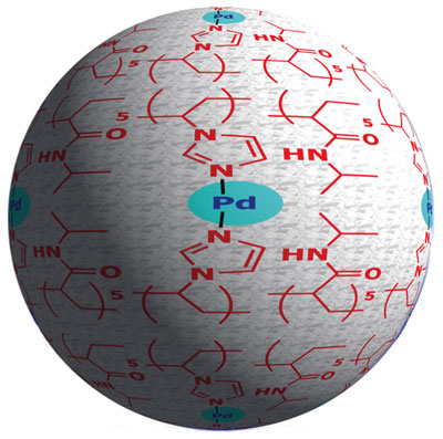
A graphical representation of the retrievable and reusable polymer–metal catalyst, showing the palladium (blue) that links two imidazole polymer units (red) through their nitrogen atoms. Copyright : 2011 Yoichi Yamada


Metal-based chemical catalysts have excellent green chemistry credentials—in principle at least. In theory, catalysts are reusable because they drive chemical reactions without being consumed. In reality, however, recovering all of a catalyst at the end of a reaction is difficult, so it is gradually lost. Now, chemists can retain, retrieve, and reuse metal catalysts by trapping them with a polymer matrix, thanks to recent work by Yoichi Yamada at the RIKEN Advanced Science Institute, Wako, Yasuhiro Uozumi at RIKEN and Japan’s Institute for Molecular Science and Shaheen Sarkar, also at RIKEN.

Attaching metal catalysts to an insoluble polymer support, which is recoverable at the end of a reaction by simple filtration, is far from a new idea. Traditionally, chemists attached their metal catalyst to an insoluble polymer resin. However, the metal invariably leached out of the polymer over time so the catalysts were still slowly lost.

Yamada and his colleagues' approach, in contrast, integrated the metal into the polymer matrix, which trapped it much more effectively. The researchers achieved this level of integration by starting with a soluble polymer precursor instead of an insoluble resin. This material contains imidazole units, a chemical structure known to bind strongly to metals such as palladium. An insoluble composite material formed only after the researchers added palladium to the mixture because it causes the imidazole units to self-assemble around atoms of the metal—a process that they call 'molecular convolution'.

Scanning electron microscopy revealed that the resulting polymer–palladium globules ranged from 100 to 1,000 nm in diameter, which aggregated into a highly porous structure reminiscent of a tiny bathroom sponge. "This sponge-like insoluble material can easily capture substrates and reactants from the solution, which readily react with metal species embedded in the sponge," says Yamada.

The researchers showed that the catalyst is highly active as well as reusable; it is the most active catalyst yet reported for a carbon–carbon bond-forming reaction known as an allylic arylation. They also reused the catalyst multiple times with no apparent loss of activity, and detected no leaching of palladium from the polymer into the reaction mixture.

Yamada and colleagues are now developing a range of composite catalysts incorporating different metals that can catalyze many other kinds of reactions. "These extremely highly active and reusable catalysts will provide a safe and highly efficient chemical process, which we hope will be adopted for industrial chemical process," Yamada says.

Source: RIKEN

Additional Information:

Project to pour water into volcano to make power

Engineerblogger
Jan 16, 2011

In this May 16, 2008, file photo, Newbery Crater project drilling manager Fred Wilson stands near a drilling rig at the Newberry Crater geothermal project as he describes the work near LaPine, Ore. Geothermal energy developers plan to pump 24 million gallons of water into the side of the dormant Central Oregon volcano this summer to demonstrate new technology they hope will give a boost to a green energy sector that has yet to live up to its promise. (AP Photo/Don Ryan, File)

Geothermal energy developers plan to pump 24 million gallons of water into the side of a dormant volcano in Central Oregon this summer to demonstrate new technology they hope will give a boost to a green energy sector that has yet to live up to its promise.

They hope the water comes back to the surface fast enough and hot enough to create cheap, clean electricity that isn't dependent on sunny skies or stiff breezes—without shaking the earth and rattling the nerves of nearby residents.

Renewable energy has been held back by cheap natural gas, weak demand for power and waning political concern over global warming. Efforts to use the earth's heat to generate power, known as geothermal energy, have been further hampered by technical problems and worries that tapping it can cause earthquakes.

Even so, the federal government, Google and other investors are interested enough to bet $43 million on the Oregon project. They are helping AltaRock Energy, Inc. of Seattle and Davenport Newberry Holdings LLC of Stamford, Conn., demonstrate whether the next level in geothermal power development can work on the flanks of Newberrry Volcano, located about 20 miles south of Bend, Ore.

"We know the heat is there," said Susan Petty, president of AltaRock. "The big issue is can we circulate enough water through the system to make it economic."

The heat in the earth's crust has been used to generate power for more than a century. Engineers gather hot water or steam that bubbles near the surface and use it to spin a turbine that creates electricity. Most of those areas have been exploited. The new frontier is places with hot rocks, but no cracks in the rocks or water to deliver the steam.

To tap that heat—and grow geothermal energy from a tiny niche into an important source of green energy—engineers are working on a new technology called Enhanced Geothermal Systems.

"To build geothermal in a big way beyond where it is now requires new technology, and that is where EGS comes in," said Steve Hickman, a research geophysicist with the U.S. Geological Survey in Menlo Park, Calif.

Wells are drilled deep into the rock and water is pumped in, creating tiny fractures in the rock, a process known as hydroshearing.

Cold water is pumped down production wells into the reservoir, and the steam is drawn out.
Hydroshearing is similar to the process known as hydraulic fracturing, used to free natural gas from shale formations. But fracking uses chemical-laden fluids, and creates huge fractures. Pumping fracking wastewater deep underground for disposal likely led to recent earthquakes in Arkansas and Ohio.

Fears persist that cracking rock deep underground through hydroshearing can also lead to damaging quakes. EGS has other problems. It is hard to create a reservoir big enough to run a commercial power plant.

Progress has been slow. Two small plants are online in France and Germany. A third in downtown Basel, Switzerland, was shut down over earthquake complaints. A project in Australia has had drilling problems.

A new international protocol is coming out at the end of this month that urges EGS developers to keep projects out of urban areas, the so-called "sanity test," said Ernie Majer, a seismologist with the Lawrence Berkeley National Laboratory. It also urges developers to be upfront with local residents so they know exactly what is going on.

AltaRock hopes to demonstrate a new technology for creating bigger reservoirs that is based on the plastic polymers used to make biodegradable cups.

It worked in existing geothermal fields. Newberry will show if it works in a brand new EGS field, and in a different kind of geology, volcanic rock, said Colin Williams, a USGS geophysicist also in Menlo Park.
The U.S. Department of Energy has given the project $21.5 million in stimulus funds. That has been matched by private investors, among them Google with $6.3 million.

Majer said the danger of a major quake at Newbery is very low. The area is a kind of seismic dead zone, with no significant faults. It is far enough from population centers to make property damage unlikely. And the layers of volcanic ash built up over millennia dampen any shaking.

But the Department of Energy will be keeping a close eye on the project, and any significant quakes would shut it down at least temporarily, he said. The agency is also monitoring EGS projects at existing geothermal fields in California, Nevada and Idaho.

"That's the $64,000 question," Majer said. "What's the biggest earthquake we can have from induced seismicity that the public can worry about."

Geologists believe Newberry Volcano was once one of the tallest peaks in the Cascades, reaching an elevation of 10,000 feet and a diameter of 20 miles. It blew its top before the last Ice Age, leaving a caldera studded with towering lava flows, two lakes, and 400 cinder cones, some 400 feet tall.

Although the volcano has not erupted in 1,300 years, hot rocks close to the surface drew exploratory wells in the 1980s.

Over 21 days, AltaRock will pour 800 gallons of water per minute into the 10,600-foot test well, already drilled, for a total of 24 million gallons. According to plan, the cold water cracks the rock. The tiny plastic particles pumped down the well seal off the cracks. Then more cold water goes in, bypassing the first tier, and cracking the rock deeper in the well. That tier is sealed off, and cold water cracks a third section. Later, the plastic melts away.

Seismic sensors produce detailed maps of the fracturing, expected to produce a reservoir of cracks starting about 6,000 feet below the surface, and extending to 11,000 feet. It would be about 3,300 feet in diameter.

The U.S. Bureau of Land Management released an environmental assessment of the Newberry project last month that does not foresee any problems that would stop it. The agency is taking public comments before making a final decision in coming months.

No power plant is proposed, but one could be operating in about 10 years, said Doug Perry, president and CEO of Davenport Newberry.

EGS is attractive because it vastly expands the potential for geothermal power, which, unlike wind and solar, produces power around the clock in any weather.

Natural geothermal resources account for about 0.3% of U.S. electricity production, but a 2007 Massachusetts Institute of Technology report projected EGS could bump that to 10% within 50 years, at prices competitive with fossil-fuels.

Few people expect that kind of timetable now. Electricity prices have fallen sharply because of low natural gas prices and weak demand brought about by the Great Recession and state efficiency programs.

But the resource is vast. A 2008 USGS assessment found EGS throughout the West, where hot rocks are closer to the surface than in the East, has the potential to produce half the country's electricity.

"The important question we need to answer now," said Williams, the USGS geophysicist who compiled the assessment, "is how geothermal fits into the renewable energy picture, and how EGS fits. How much it is going to cost, and how much is available."

Source: The Associated Press

Magnetic Memory Miniaturized to Just 12 Atoms

Technology Review
Jan 16, 2012


This scanning tunneling microscope image shows a group of 12 iron atoms, the smallest magnetic memory bit ever made. Credit: IBM


The smallest magnetic-memory bit ever made—an aggregation of just 12 iron atoms created by researchers at IBM—shows the ultimate limits of future data-storage systems.

The magnetic memory elements don't work in the same way that today's hard drives work, and, in theory, they can be much smaller without becoming unstable. Data-storage arrays made from these atomic bits would be about 100 times denser than anything that can be built today. But the 12 atoms making up each bit must be painstakingly assembled using an expensive and complex microscope, and the bits can hold data for only a few hours and at low temperatures approaching absolute zero, so the miniscule memory elements won't be found in consumer devices anytime soon.

As the semiconductor industry bumps up against the limits of scaling by making memory and computation devices ever smaller, the IBM Almaden research group, led by Andreas Heinrich, is working from the other end, building computing elements atom-by-atom in the lab.

The necessary technology for large-scale manufacturing at the single-atom scale doesn't exist yet. Today, says Heinrich, the question is, "What is it you would want to build on the scale of atoms for data storage and computation, in the distant future?"

As engineers miniaturize conventional devices, they're finding that quantum physics, which never had to be accounted for in the past, makes devices less stable. As conventional magnetic memory bits are miniaturized, for example, each bit's magnetic field begins to affect its neighbors', weakening each bit's ability to hold on to a 1 or a 0.

The IBM researchers found that it was possible to sidestep this problem by using groups of atoms that display a different kind of magnetism. The key, says Heinrich, is the magnetic spin of each individual atom.
To read more click here...

One step closer to controlling nuclear fusion

Engineerblogger
Jan 16, 2012


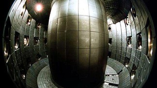
Confined chamber for the plasma © EPFL

Using a heating system, physicists have succeeded for the first time in preventing the development of instabilities in an efficient alternative way relevant to a future nuclear fusion reactor. It’s an important step forward in the effort to build the future ITER reactor.

Scientists have achieved a milestone: they have managed to stop the growth of instabilities inside a nuclear fusion reactor. How? Here’s a look at this energy source, which despite being challenging to control, is nevertheless extremely promising.

Nuclear fusion is an attempt to reproduce the energy of the Sun in an Earth-based reactor system. When gas is heated to several million degrees, it becomes plasma. Sometimes in the plasma, an instability will appear and grow large enough to perturb the plasma, making it vibrate despite the presence of the magnetic field in which it is contained. If the plasma touches the walls of the reactor, it will cool rapidly and create large electromagnetic forces within the structure of the machine.

The challenge is to reduce the instabilities deep within in the interior of the plasma so that they don’t amplify, while at the same time allowing the reactor to continue to function normally. Thus it is necessary to work within the specific configuration of these fusion reactors, where the plasma is strongly confined by a magnetic field. By adjusting an antenna that emits electromagnetic radiation, Jonathan Graves and his colleagues from EPFL’s Center for Research in Plasma Physics were able to quench the instabilities when they appear, in the precise region where they are forming, and without perturbing the rest of the installation.

From theory to practice

The physicists first conducted simulations to verify the extent to which specific radiation frequencies and locations of application would suppress the growth of instabilities. Then they carried out tests to confirm their calculations. The beauty of their approach is that they were able to use antennas that are used as part of the system to heat the plasma, and that are already present in the Joint European Torus (JET), the largest reactor currently in use. Surprisingly, the simulations and the tests showed that heating and instability suppression can be combined, by aiming the radiation slightly off-center in the plasma.

The next step will be to add a detector system that will make it possible to neutralize instabilities in real time over longer time periods. These improvements can then be implemented in the ITER fusion reactor, currently in development in Southern France.

Source: École polytechnique fédérale de Lausanne (EPFL)

Additional Information:

Friday, January 13, 2012

"Open-source" robotic surgery platform going to top medical research labs

Engineerblogger
Jan 12, 2012


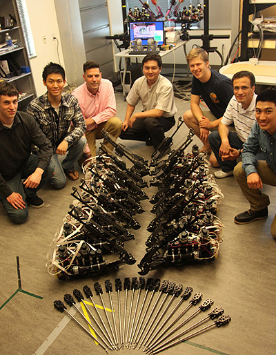
Team members posed with components of the Raven II surgical robotic systems developed in the Bionics Lab at the Baskin School of Engineering. From left to right: Zachary Wells (bioengineering undergraduate), Calvin Yoo (bioengineering undergraduate), lab director Jacob Rosen (associate professor of computer engineering), Ji Ma (postdoctoral researcher), Joshua Schloemer (economics undergraduate), Farhad Ighani (computer engineering undergraduate), and Kyle Fujisawa (computer engineering undergraduate). (Photo by Carolyn Lagattuta)


Robotics experts at UC Santa Cruz and the University of Washington (UW) have completed a set of seven advanced robotic surgery systems for use by major medical research laboratories throughout the United States. After a round of final tests, five of the systems will be shipped to medical robotics researchers at Harvard University, Johns Hopkins University, University of Nebraska, UC Berkeley, and UCLA, while the other two systems will remain at UC Santa Cruz and UW.

"We decided to follow an open-source model, because if all of these labs have a common research platform for doing robotic surgery, the whole field will be able to advance more quickly," said Jacob Rosen, associate professor of computer engineering in the Baskin School of Engineering at UCSC and principal investigator on the project.

Rosen and Blake Hannaford, director of the UW Biorobotics Laboratory, lead the research groups that developed the Raven II robotic surgery system and its predecessor, Raven I. A grant from the National Science Foundation funded their work to create seven identical Raven II systems. Hannaford said the systems will be shipped out from UW by the end of January. After they are delivered and installed, all seven systems will be networked together over the Internet for collaborative experiments.

Robotic surgery has the potential to enable new surgical procedures that are less invasive than existing techniques. For some procedures, such as prostate surgery, the use of surgical robots is already standard practice. In addition, telesurgery, in which the surgeon operates a robotic system from a remote location, offers the potential to provide better access to expert care in remote areas and the developing world. Having a network of laboratories working on a common platform will make it easier for researchers to share software, replicate experiments, and collaborate in other ways.

Even though it meant giving competing laboratories the tools that had taken them years to develop, Rosen and Hannaford decided to share the Raven II because it seemed like the best way to move the field forward. "These are the leading labs in the nation in the field of surgical robotics, and with everyone working on the same platform we can more easily share new developments and innovations," Hannaford said.

According to Rosen, most research on surgical robotics in the United States has focused on developing new software for various commercially available robotic systems. "Academic researchers have had limited access to these proprietary systems. We are changing that by providing high-quality hardware developed within academia. Each lab will start with an identical, fully-operational system, but they can change the hardware and software and share new developments and algorithms, while retaining intellectual property rights for their own innovations," Rosen said.

The Raven II includes a surgical robot with two robotic arms, a camera for viewing the operational field, and a surgeon-interface system for remote operation of the robot. The system is powerful and precise enough to support research on advanced robotic surgery techniques, including online telesurgery.

In addition to Rosen and Hannaford, UCSC postdoctoral researchers Daniel Glozman and Ji Ma, along with a group of dedicated undergraduate students working in Rosen's Bionics Lab, played a key role in developing the Raven II. Rosen and Glozman have also developed a Raven IV surgical robotics system, which includes four robotic arms and two cameras. The system enables collaboration between two surgeons working from separate locations and connected over the Internet.

Source: University of California - Santa Cruz

Optical nanoantennas enable efficient multipurpose particle manipulation

Engineerblogger
Jan 13, 2012


Concept art depicting the various potential BNA trapping states

University of Illinois researchers have shown that by tuning the properties of laser light illuminating arrays of metal nanoantennas, these nano-scale structures allow for dexterous optical tweezing as well as size-sorting of particles.

"Nanoantennas are extremely popular right now because they are really good at concentrating optical fields in small areas,” explained Kimani Toussaint, Jr., an assistant professor of mechanical science and engineering at the University of Illinois at Urbana-Champaign. “In this work, we demonstrate for the first time the use of arrays of gold Bowtie Nanoantenna Arrays (BNAs) for multipurpose optical trapping and manipulation of submicrometer- to micrometer-sized objects. We think that this could be a fruitful area to pursue, particularly because of the growing interest in lab-on-a-chip devices.”

According to the researchers, the excellent field enhancement and confinement properties of BNAs enable highly efficient, optical tweezers which permit high-speed manipulation of submicrometer to micrometer-sized objects in aqueous environments using remarkably low-input power densities. These characteristics could be useful for optofluidic applications (e.g., lab-on-a-chip devices), manipulating biological matter with reduced specimen photo damage, formation of optical matter, and basic physics studies of colloidal dynamics.

“In contrast to other plasmonic tweezers, we find that BNAs permit particle trapping, manipulation and sorting utilizing only the optical parameter space, namely, low input power densities, wavelength and polarization,” said Brian Roxworthy, a graduate student in Toussaint’s research group and first author on the paper, “Application of Plasmonic Bowtie Nanoantenna Arrays for Optical Trapping, Stacking, and Sorting,” which appears in the journal Nano Letters.

Using empirically obtained “optical trapping phase diagrams” to achieve the desired trapping response, the researchers demonstrated several types of particle manipulation, including single-beam optical tweezing of single particles over the entire nanoantenna area, single-beam optical tweezing of 2D hexagonal packed particles over the entire nanoantenna area, and optical sorting of particles by size; stacking of submicron to micron-sized particles in 3D.

According to Toussaint, this is the first demonstration of a range of particle manipulation behavior for a given nanoantenna array.
“We actually excite our nanoantennas off resonance, which to our knowledge is a first, and at the right input optical power, we take advantage of thermal effects combined with optical forces to enable tweezing of tens of particles at a time,” Toussaint explained. “We show that very low power densities are required to achieve the aforementioned behavior. For example, we were able to carry out experiments using a standard laser pointer.”

In addition to Toussaint, the lead investigator for the project, co-investigators include Gang Logan Liu, an assistant professor of electrical and computer engineering at Illinois, and former Illinois faculty member Nicholas Fang, who is now at the Massachusetts Institute of Technology.

Source: University of Illinois at Urbana-Champaign

Additional Information:

Magnetic actuation enables nanoscale thermal analysis

Engineerblogger
Jan 13, 2012


Atomic force microscope with integrated heater actuated using Lorentz force

Polymer nano-films and nano-composites are used in a wide variety of applications from food packaging to sports equipment to automotive and aerospace applications. Thermal analysis is routinely used to analyze materials for these applications, but the growing trend to use nanostructured materials has made bulk techniques insufficient.

In recent years an atomic force microscope-based technique called nanoscale thermal analysis (nanoTA) has been employed to reveal the temperature-dependent properties of materials at the sub-100 nm scale. Typically, nanothermal analysis works best for soft polymers. Researchers at the University of Illinois at Urbana-Champaign and Anasys Instruments, Inc. have now shown that they can perform nanoscale thermal analysis on stiff materials like epoxies and filled composites.

“This new technique lets us measure temperature and frequency-dependent properties of materials rapidly over a wide bandwidth,” noted William King, the College of Engineering Bliss Professor in the Department of Mechanical Science and Engineering at Illinois, who led the research. The technique works by flowing a current around the U-shaped arms of a self-heating atomic force microscope (AFM) cantilever and interacting that current with a magnetic field. The magnetic field allows the tip-sample force to be modulated right near the tip of the AFM.

“We are able to achieve nanometer-scale force control that is independent from the heating temperature,” according to Byeonghee Lee, first author of the paper.

“Conventional nanothermal analysis has struggled with highly filled, highly crosslinked materials and sub-100 nm thin films. This new technique has allowed us to reliably measure and map glass transitions and melting transions on classes of materials that were previously very challenging,” said Craig Prater, chief technology officer at Anasys Instruments and co-author on the paper.


The research was performed in King’s Nanoengineering Laboratory and at Anasys Instruments. King is also affiliated with the Department of Materials Science and Engineering, the Department of Electrical and Computer Engineering, the Beckman Institute for Advanced Science and Technology, the Micro and Nanotechnology Laboratory, and the Materials Research Laboratory, all at the University of Illinois. The research was sponsored by the Air Force Office of Scientific Research and the National Science Foundation.

Source:  University of Illinois at Urbana-Champaign

Additional Information:

Send in the Supplies: RoboCopters in Marines’ Future

Engineerblogger
Jan 13, 2012


Marines running low on ammo may one day use an app on their digital handhelds to summon a robotic helicopter to deliver supplies within minutes, enabled by technologies from a new Office of Naval Research (ONR) program.

The Autonomous Aerial Cargo Utility System (AACUS) is a five-year, $98 million effort to develop sensors and control technologies for robotic vertical take-off and landing aircraft.

“AACUS is a leap-ahead technology that allows the Navy and the Marine Corps to move beyond having a highly trained operator fly an unmanned aircraft,” said Rear Adm. Matthew Klunder, chief of naval research. “The program will let us leverage advanced autonomy, but still maintain the central and critical role of the human operator as the supervisor.”

Marines based at outposts or in the field will be able to request the autonomous cargo helicopters for rapid resupply of combat essentials.

“We want to turn any helicopter into a logistics machine,” said Dr. Mary “Missy” Cummings, program officer for AACUS, ONR’s newest innovative naval prototype. “In the near term, we want to succeed in fully-autonomous landings in austere locations, so Marines can get whatever they need on demand.

“In the long term, this could be a real life saver and revolutionize first response,” she added. While rapid resupply is the immediate focus for AACUS, long-term applications could include critical medical missions such as casualty evacuation.

Program officials are seeking researchers who will develop threat- and obstacle-detection and avoidance systems, as well as autonomous landing capabilities that can operate across different types of aircraft. They expect teams from industry and academia to join forces to compete for the contracts.

Proposals are due Feb. 22. Officials plan to award up to two contracts in April.

The effort follows the Marine Corps Warfighting Laboratory’s successful program to develop an unmanned system capable of hauling cargo semi-autonomously to landing zones at bases. The prototype, called K-MAX, flew its first combat mission in Afghanistan in mid-December, resupplying Marines with cargo carried in a sling-load.

AACUS, on the other hand, is aimed at internal load-carrying capacity. It will be a major leap ahead in autonomy, said Cummings. While K-MAX requires a trained operator within line-of-sight to fly, any operator will be able to call for AACUS from any location.

“It’s going to be designed to work with people who have no flight experience,” she said. “An operator will pick up his iPad or Android and make an emergency supply request. He’ll request that the helicopter come to him and land as close to him as possible.”

The helicopter not only will take off by itself, but will plan its own flight path and navigate its way through the airspace, requiring little to no input from an operator other than to verify its proposed landing site. The concept will require improvement in data processing.

“How you take the data from sensors and integrate them to make these decisions—that’s one of the big leaps,” said Cummings. “It’s like putting a frontal lobe on the helicopter.”

For more information on submitting proposals, review the AACUS broad agency announcement (12-004).

Source:  Office of Naval Research 

Related Information:

Team Designs New Nanotech Technique for Lower-Cost Materials Repair

Engineerblogger
Jan 13, 2011


A recent materials repair discovery validates prior theory and may lead to significant conservation of material in diagnosing and repairing structural damage. The cartoon illustrates how nanoparticle-containing capsules roll or glide over damaged substrates, selectively depositing their nanoparticle contents into fractures. Illustration courtesy of Todd Emrick, UMass Amherst


 In the super-small world of nanostructures, a team of polymer scientists and engineers at the University of Massachusetts Amherst have discovered how to make nano-scale repairs to a damaged surface equivalent to spot-filling a scratched car fender rather than re-surfacing the entire part. The work builds on a theoretical prediction by chemical engineer and co-author Anna Balazs at the University of Pittsburgh.

Their discovery is reported this week in the current issue of Nature Nanotechnology. The new technique has many practical implications, especially that repairing a damaged surface with this method would require significantly smaller amounts of material, avoiding the need to coat entire surfaces when only a tiny fraction is cracked, says team leader and UMass Amherst polymer scientist Todd Emrick.

"This is particularly important because even small fractures can then lead to structural failure but our technique provides a strong and effective repair. The need for rapid, efficient coating and repair mechanisms is pervasive today in everything from airplane wings to microelectronic materials to biological implant devices," he adds.

At nano-scale, damaged areas typically possess characteristics quite distinct from their undamaged surrounding surface, including different topography, wetting characteristics, roughness and even chemical functionality, Emrick explains. He adds, "Anna Balazs predicted, using computer simulation, that if nanoparticles were held in a certain type of microcapsule, they would probe a surface and release nanoparticles into certain specific regions of that surface," effectively allowing a spot-repair.

This vision of capsules probing and releasing their contents in a smart, triggered fashion, known as "repair-and-go," is characteristic of biological process, such as in white blood cells, Emrick adds.

He says the experimental work to support the concept required insight into the chemistry, physics and mechanical aspects of materials encapsulation and controlled release, and was achieved by collaboration among three polymer materials laboratories at UMass Amherst, led by Alfred Crosby, Thomas Russell and himself.

The researchers show how using a polymer surfactant stabilizes oil droplets in water (in emulsion droplets or capsules), encapsulating nanoparticles efficiently, but in a manner where they can be released when desired, since the capsule wall is very thin.

"We then found that the nanoparticle-containing capsules roll or glide over damaged substrates, and very selectively deposit their nanoparticle contents into the damaged (cracked) regions. Because the nanoparticles we use are fluorescent, their localization in the cracked regions is clearly evident, as is the selectivity of their localization."

Using rapid and selective deposition of sensor material in damaged regions, their innovative work also provides a precise method for detecting damaged substrates, he stresses. Finally, the new encapsulation techniques allow delivery of hydrophobic objects in a water-based system, further precluding the need for organic solvents in industrial processes that are dis-advantageous from an environmental standpoint.

Emrick says, "Having realized the concept experimentally, looking forward we now hope to demonstrate recovery of mechanical properties of coated objects by adjusting the composition of the nanoparticles being delivered."

The work was supported by the National Science Foundations’ (NSF) Materials Research Science and Engineering Center on Polymers at UMass Amherst, an NSF Integrative Graduate Education and Research Traineeship (IGERT) award, the NSF Center for Hierarchical Manufacturing, the U.S. Department of Energy and its Office of Basic Energy Science.

Source:  University of Massachusetts Amherst

Algae for your fuel tank: New process for producing biodiesel from microalgae oil

Engineerblogger
Jan 13, 2012

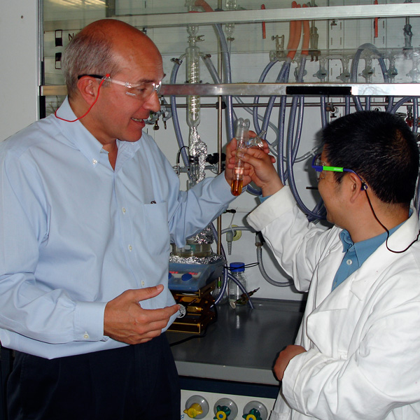
Prof. Lercher with a scientist of his team - Photo: Battenberg/TUM

 The available amount of fossil fuels is limited and their combustion in vehicle motors increases atmospheric CO2 levels. The generation of fuels from biomass as an alternative is on the rise. In the journal Angewandte Chemie, Johannes A. Lercher and his team at the Technische Universitaet Muenchen have now introduced a new catalytic process that allows the effective conversion of biopetroleum from microalgae into diesel fuels.

Plant oils from sources such as soybean and rapeseed are promising starting materials for the production of biofuels. Microalgae are an interesting alternative to these conventional oil-containing crops. Microalgae are individual cells or short chains of cells from algae freely moving through water. They occur in nearly any pool of water and can readily be cultivated. “They have a number of advantages over oil-containing agricultural products,” explains Lercher. “They grow significantly faster than land-based biomass, have a high triglyceride content, and, unlike the terrestrial cultivation of oilseed plants, their use for fuel production does not compete with food production.”

Previously known methods for refining oil from microalgae suffer from various disadvantages. The resulting fuel either has too high an oxygen content and poor flow at low temperatures, or a sulfur-containing catalyst may contaminate the product. However, other catalysts are still not efficient enough. The Munich scientists now propose a new process, for which they have developed a novel catalyst: nickel on a porous support made of zeolite HBeta. They have used this to achieve the conversion of raw, untreated algae oil under mild conditions (260 °C, 40 bar hydrogen pressure). Says Lercher: “The products are diesel-range saturated hydrocarbons that are suitable for use as high-grade fuels for vehicles.”

The oil produced by the microalgae is mainly composed of neutral lipids, such as mono-, di-, and triglycerides with unsaturated C18 fatty acids as the primary component (88 %). After an eight-hour reaction, the researchers obtain 78 % liquid alkanes with octadecane (C18) as the primary component. The main gas-phase side products are propane and methane.

Analysis of the reaction mechanism shows that this is a cascade reaction. First the double bonds of the unsaturated fatty acid chains of the triglycerides are saturated by hydrogen. Then, the now saturated fatty acids take up hydrogen and are split from their glycerin component, which reacts to form propane. In the final step, the acid groups in the fatty acids are reduced stepwise to the corresponding alkane.

Source:   Technische Universitaet Muenchen 

Additional Information:
  • Towards Quantitative Conversion of Microalgae Oil to Diesel-Range Alkanes with Bifunctional Catalysts, B. Peng, Y. Yao, C. Zhao und J.A. Lercher,  Angewandte Chemie, 2011 – Doi: 10.1002/ange.201106243