Pages

Subscribe:

Ads 468x60px

Showing posts with label Technology. Show all posts

Friday, February 3, 2012

Mitsubishi Electric Announces New Ultra-High-Speed Elevator Technologies

Engineerblogger
Feb 3, 2012

Shanghai Tower will represent China's dynamic 'future

Mitsubishi Electric Corporation announced today its new suite of technologies that enable ultra-high-speed elevators to travel faster than 1,000 meters per minute, or 60 kph, with enhanced efficiency, comfort and safety. The technologies will be incorporated in the world's fastest elevators, including those developed by Mitsubishi Electric for the 632-meter Shanghai Tower under construction in Shanghai, China.

In response to the increasing height of high-rise buildings amid continuing urban population growth, the role of elevators is gaining even greater importance. In response, Mitsubishi Electric is developing advanced solutions incorporating technologies and equipment for enhanced drive and controllability, safety, super high-rise cable mechanics and passenger comfort. The company's new suite of ultra-high-speed elevator technologies includes the following advancements:

1.  Drive and Controllability
  • The traction motor incorporates a permanent magnetic motor for energy-efficient, low-noise, low-vibration operation.
  • A single motor has two grouped three-phase winding coils and parallel drive systems controlled by separate control panels. Each motor has a built-in converter to regenerate electricity, lowering power consumption by more than 30 percent.
  • Brakes composed of two units with a hydraulic driven clamp-type disk brake achieve stable braking.
 
2.  Safety

  • Safety gears, which activate the brakes by grasping the guide rails in emergencies if cables become transected, comprise two stages to manage increased kinetic energy due to ultra-high speeds.
  • Fine ceramic is used for the safety gear shoe to realize high resistance to heat, abrasion and shock. Braking is extra-stable even if high frictional heat is generated when the safety gear is activated.
  • The hydraulic oil buffer (shock absorber) at the bottom of the elevator shaft has an advanced plunger comprising three stages for exceptional shock absorption within a shortened frame.
  • Newly developed governor monitors elevator speed stably even with heavy loads placed by ropes traveling at high speeds over long distances.

3.  Super high-rise cable mechanics

  • A steel core with a wider diameter provides high intensity, allowing traveling cables to be lightened by using lightweight sheath material and operated by a highly efficient electric power carrier system.
  • Mitsubishi Electric's new "sfleX-rope" comprising bundles of high-intensity steel wire strands, each covered with plastic, offers higher intensity than conventional rope for safe operation despite the greater weight of longer ropes. Each wire has a higher density and wider cross-sectional area than conventional rope, which helps to reduce rope stretching caused when passengers step onto the elevator.


4.  Ride comfort
  •   A new active roller guide, which reduces vibration from the guide rails and wind, enhances passenger comfort even at ultra-high speeds.
  •   The inside of the car is extra-quiet thanks to a streamlined aerodynamic car cover and a high sound insulation cage.
  • Air pressure control helps to minimize rapid changes in atmospheric pressure for reduced ear discomfort.

Just like cars, going that fast also leads to the question of safety – rest assured that Mitsubishi will deliver enhanced efficiency, comfort and safety as thousands of people traverse through these elevators each day. Fine ceramic is the material of choice for the safety gear shoe as it has a high resistance to heat, abrasion and shock. Never mind if high frictional heat is generated, braking remains extremely stable.

Source: Mitsubishi Electric Corporation

Graphene electronics moves into a third dimension

Engineerblogger
Feb 3, 2012


Graphene nanofabric. SEM micrograph of a strongly crumpled graphene sheet on a Si wafer. Note that it looks just like silk thrown over a surface. Lateral size of the image is 20 microns. Si wafer is at the bottom-right corner. Credit: University of Manchester

In a paper published this week in Science, a Manchester team lead by Nobel laureates Professor Andre Geim and Professor Konstantin Novoselov has literally opened a third dimension in graphene research. Their research shows a transistor that may prove the missing link for graphene to become the next silicon.

Graphene – one atomic plane of carbon – is a remarkable material with endless unique properties, from electronic to chemical and from optical to mechanical.

One of many potential applications of graphene is its use as the basic material for computer chips instead of silicon. This potential has alerted the attention of major chip manufactures, including IBM, Samsung, Texas Instruments and Intel. Individual transistors with very high frequencies (up to 300 GHz) have already been demonstrated by several groups worldwide.

Unfortunately, those transistors cannot be packed densely in a computer chip because they leak too much current, even in the most insulating state of graphene. This electric current would cause chips to melt within a fraction of a second.

This problem has been around since 2004 when the Manchester researchers reported their Nobel-winning graphene findings and, despite a huge worldwide effort to solve it since then, no real solution has so far been offered.

The University of Manchester scientists now suggest using graphene not laterally (in plane) – as all the previous studies did – but in the vertical direction. They used graphene as an electrode from which electrons tunnelled through a dielectric into another metal. This is called a tunnelling diode.

Then they exploited a truly unique feature of graphene – that an external voltage can strongly change the energy of tunnelling electrons. As a result they got a new type of a device – vertical field-effect tunnelling transistor in which graphene is a critical ingredient.

Dr Leonid Ponomarenko, who spearheaded the experimental effort, said: “We have proved a conceptually new approach to graphene electronics. Our transistors already work pretty well. I believe they can be improved much further, scaled down to nanometre sizes and work at sub-THz frequencies.”

“It is a new vista for graphene research and chances for graphene-based electronics never looked better than they are now”, adds Professor Novoselov.

Graphene alone would not be enough to make the breakthrough. Fortunately, there are many other materials, which are only one atom or one molecule thick, and they were used for help.

The Manchester team made the transistors by combining graphene together with atomic planes of boron nitride and molybdenum disulfide. The transistors were assembled layer by layer in a desired sequence, like a layer cake but on an atomic scale.

Such layer-cake superstructures do not exist in nature. It is an entirely new concept introduced in the report by the Manchester researchers. The atomic-scale assembly offers many new degrees of functionality, without some of which the tunnelling transistor would be impossible.

“The demonstrated transistor is important but the concept of atomic layer assembly is probably even more important,” explains Professor Geim.

Professor Novoselov added: “Tunnelling transistor is just one example of the inexhaustible collection of layered structures and novel devices which can now be created by such assembly.

“It really offers endless opportunities both for fundamental physics and for applications. Other possible examples include light emission diodes, photovoltaic devices, and so on.”

Source: University of Manchester

Additional Information:

Tuesday, January 31, 2012

Device Could Drive Down Solar's Cost

Technology Review
Jan 31, 2012
 
Power play: Inverters mounted to the bottom of each panel provide grid-ready power at a test site in Sunnyvale, California. Credit: ArrayPower

As solar panel manufacturers try to harvest more of the sun's energy for less, they face increasingly diminishing returns. At roughly $1 per watt, the cost of solar modules now represents less than a third of the total cost of commercial solar installations. To cut the total cost of solar power—currently $3.00 to $3.50 per watt—bigger gains will have to come from improvements in the power electronics, wiring, and mounting systems required for solar installations.

ArrayPower, a startup based in Sunnyvale, California, has developed a new type of solar inverter—the device that converts direct current (DC) power produced by solar panels to grid-ready, alternating current (AC) electricity—that it claims could significantly reduce the cost of solar power. The company says its "sequenced inverter" will reduce the cost of commercial solar by 35 cents per watt, or more than 10 percent, by lowering capital costs, simplifying installation, and increasing output.

Large-scale solar installations currently use either a single "central" inverter or a number of "string" inverters to convert power from groups of panels strung together in series. Both approaches, however, suffer from low efficiencies because of the way the panels are connected. In either scenario, if one panel is damaged or shaded from the sun, the system's entire output is diminished to the level of its lowest-producing panel.

ArrayPower seeks to maximize power output through a new type of inverter mounted to each panel. The device is similar to microinverters now used in residential solar installations. By converting DC to AC power at each module, microinverters maximize the power output of each module, thereby increasing system output by roughly 3 percent to 10 percent.

Microinverters are typically more expensive because they require sophisticated electronics to filter and smooth the alternating current coming out of each inverter. A major cost is an electrolytic capacitor, essentially a chemical battery that stores energy for short bursts, allowing the inverter to send out pulses of electricity that create an alternating current. Further, microinverters typically only yield single-phase AC electricity, an electric current that is suited for residential use but not commercial or utility use.
To read more click here...

Monday, January 30, 2012

New Capabilities of today’s Automotive Glass Equipment

Engineerblogger
Jan 30, 2012


Today’s know-how, together with new developments in control technology and machine production technologies allow to utilise automotive glass grinding and cutting machines in new ways.

This equipment with its more flexible use, can reach higher quality and/or much shorter cycle times as well as it is open for new applications.

New equipment with direct drive technology is able to preprocess glass in a higher quality and at the same time faster than in the past. Thanks to the drives the gearboxes can be eliminated, higher torque can be achieved and higher resolution encoders can be used. Eliminating the gearboxes menas eliminating the mechanical play totally. The accuracy is given by the measurement system and the performance of the drive regulator. The measurement systems can resolve down to micrometers or micronarcs for polar systems.

Using the new technology the customers do not have to decide between productivity and quality to a given price. The new controls allow to adapt the production quality to the desired level. For example a customer can start its venture in the less demanding replacement segment, where high output is critical. If he is looking for new opportunities later it is possible to reprogram the machine to the highest quality levels. The customer is able to compete on the highest quality levels which allow asking for a higher price for the manufactured product. Todays new electronic developments allow an easy and riskless adaption of parameters. The technology, accuracy and flexibility can be applied in other glass production fields like solar or architectural production as well.


Technical basis of champ’speed
Working with two cutting bridges allows to separate relief cuts and form cuts. Furthermore the customer can separate cutting and breaking if needed. Using the correct combination distributing the processes allows moving the bottleneck process in cutting and grinding from the cutting/breaking into the grinding operation. The best combination depends on the design of the end product. In most of the cases the best solution is to do the relieve cuts on the first station and the cutting and breaking on the second station. Having two independent cutting heads with one breaking ball head gives room for the very best possible combination to increase the quality and accuracy to the maximum with the lowest possible cycle time.


Figure 1: Example windscreen

Producing a form with an accuracy of 100 percent is possible but physical parameters limit the cycle time. If needed, the machine can follow the contour exactly. This will result in a very accurate glass, but takes its time. In theory, the relation between grinding speed and forward movement should be constant. To reach a constant grinding surface the speed has to be reduced at each point where the grinding spindle makes a turn or goes around an edge. This means: the smaller the radius, the lower the speed. As the grinding wheel has a diameter, the speed of its centre point has to increase, because it has to travel a much longer way than the grinding point of the glass. In an inner arc, the travelling speed has to be reduced, because otherwise the wheel would take too much glass and will get choked.

Today there are two ways, to achieve high speed and accuracy. Firstly it is possible to make the design of the form in a way that the end result will still be in specs. This means that the design is not in the middle of the tolerance field designed, but will touch the limits with working in lower tolerance bands. The achieved result is still the same (faster production cycle, in given tolerance), but the result does not depend on factors like speed or grinding wheel diameters anymore. Secondly one can do the same like in the past i.e. opening the contour error and allow bigger deviation. But with these methods the resulting form will then depend again on process parameters like speed. This method is not recommended but is very easy to do and does not require additional know-how or skill, but the production cycle improvement can still be considerable.


Figure 2: Cutting path with new equipment can increase corner speeds, improve quality and is reproducible

Additional to the improvement in cycle time due to the higher moment of the motor, a well designed grinding path can add considerable cycle time advantages. Together with using two bridge cutting and direct drive grinders, the cycle time can come from 27 seconds for a windshield down to 16 seconds, for the same design.

Higher torque and higher accuracy allow on polar machine to increase the diameter range. Not only windshields for trucks and busses but also solar glasses or other high end glass with diagonals up to 3.6m are possible to grind with accuracies below 0.1mm around the whole circumference. This accuracy can be achieved with low cost process due to low cycle times, automotive approved equipment and low cost consumables.
 
Figure 3: Trajectory speed of the grinding wheel center

Commercial applications
The investment is not much different than in the past, but the cycle times improve a lot on the same production space. This alone can justify a replacement of machines. Higher torque motors allow running the grinders faster and more accurate. Adding the possibility to use the tolerance band in improving cycle time gives more flexibility. The decision to invest in accurate or fast equipment has not to be taken anymore. The equipment can be bought and during the time of use switched by parameters to either use the machine in a mode with very low tolerances or in a mode with very high precision.

A company can start of in producing replacement glass with very high output and low cost for example and switch for other projects to OEM manufacturing parameters with high machine and process capabilities and insuring six sigma tolerances or more. The characteristic of the equipment can cater for different markets and customers by simply pushing a button or by an intelligent design. Using this way also small companies can invest and be sure, that the equipment keeps its value for all future ventures and supports future expansions. For solar glass new dimensions of accuracy can be achieved by low costs. The flexibility is there to adjust in the future to all needs of forms or accuracy. Proven process capabilities are given out of the automotive industry.

With this equipment producing changing models is possible without making test glasses. It is possible to change from one model to the next, without wasting one glass and without tweaking parameters. Change over time is dramatically reduced and lower skilled personal can handle the machines.

Figure 4: Example of a new automotive glass preprocessing equipment – champ’speed-line of Bystronic glass

Conclusion – Limitations and things to consider
Due to the fact, that the machine does what the program defines, it means that a form has to be defined 100% correctly. The machine follows the drawing exactly. The CAD-drawing must include all detail and the transition from one drawing element to the next. Transitions of elements have to be correct and tangents have to be handled with care and accuracy. This higher demand in designing capabilities might allow to reduce the capabilities of the machine operator.

About Bystronic Glass
Bystronic glass is the most competent and reliable partner for services, machinery, plants and systems in the glass processing sector. Bystronic glass supplies its well-proven machine technologies also in important areas of the photovoltaic industry. This includes preprocessing, front-end and back-end solutions. Bystronic glass is an international brand with globally operating companies that support their customers on site and through own sales and service companies. Since 1994, Bystronic glass is part of the Conzzeta AG, a renowned Swiss industrial holding company.

Source: Glass on Web


Additional Information:

Keeping high-performance electronics cool

Engineerblogger
Jan 30, 2012


The development of sophisticated electronics using high-performance computer chips that generate much more heat than conventional chips is challenging scientists to come up with a new type of compact cooling system to keep temperatures under control.

For the past few years, a collaborative team of engineers and other scientists from academia and industry has been investigating an advanced cooling system for electric and hybrid cars as well as computers and telecommunications systems, particularly for military use in radar, lasers, and electronics in aircraft.

The technology, which is capable of handling roughly 10 times the heat generated by conventional chips, is a device, called a vapor chamber, using tiny copper spheres and carbon nanotubes to passively wick a coolant toward hot electronics, according to Suresh V. Garimella, the R. Eugene and Susie E. Goodson Distinguished Professor in the School of Mechanical Engineering at Purdue University, West Lafayette, IN.

The current thermal solution it would replace is typically a solid heat spreader using solid aluminum and copper to conduct heat, an approach inadequate for removing large amounts of heat in powerful electronics components while maintaining low operating temperatures.

A Passive System

The vapor chamber comes in the same form factor as a solid heat spreader, says Dr. Garimella, but "The working fluid contained inside continuously undergoes [evaporation] at the heat source to more efficiently remove heat than is possible by devices that rely on conduction alone."

An advantage of vapor chambers compared to other high-performance cooling technology alternatives is that a vapor chamber is a completely passive system. According to Dr. Garimella, "It can…operate continuously without any additional pumps or valves. Such passive systems are associated with high reliability. Active cooling options which allow for high heat dissipation, such as forced liquid cooling, require an external fluid flow system including a separate pump and condenser, adding to the solution cost and size."

Much of the work is being conducted at the Industry/University Cooperative Research Center's Cooling Technologies Research Center, established by Dr. Garimella at Purdue.

Integrating Nanostructures

After publishing its findings last year about the effects of conventional sintered powder copper structures on the performance of a vapor-chamber cooling technology, the team is preparing to report on the feasibility of integrating nanostructures, specifically carbon nanotubes, into the devices to further improve performance. These results and proposed techniques for integrating carbon nanotubes into vapor chambers are expected to be published in the near future, says Dr. Garimella.

"The next step is to experimentally investigate the performance enhancement provided by integration of carbon nanotubes into vapor chambers," he says. "Another critical step in converting performance enhancements observed in the lab to actual devices is to develop engineering models and methods that allow accurate prediction of device performance for specific applications."

When the program, which is being funded by the U.S. Department of Defense's Defense Advanced Research Projects Agency, is completed at the end of this year, the hope is that there will be transition to actual applications, especially for the Department of Defense, where there is significant need, says Dr. Garimella.

Source: American Society of Mechanical Engineers (ASME)

Tuesday, January 24, 2012

Europe's Driverless Car : semi-autonomous BMW car being demonstrated on a German autobahn

Technology Review
Jan 24, 2012
Easy ride: A semi-autonomous BMW car being demonstrated on a German autobahn. It can accelerate, brake, and overtake slower vehicles on its own. Credit: BMW

Tucked away in the basement of an iconic office tower shaped like four engine cylinders, engineer Werner Huber is telling me about the joy of driving. We're here at BMW headquarters, in Munich, Germany—capital of Bavaria, and arguably of driving itself. But Huber oversees strategic planning for advanced driver assistance systems, so in a way, his job is to put an end to driving—at least as we know it.

"I think that in 10 to 15 years, it could be another world," Huber says. He's not willing to predict exactly what driving will look like then, but he's certain humans will be doing a lot less of it.

For many people, automated cars call to mind those high-tech vehicles with a rotating periscope on top that Google has been driving around California. But Huber and executives at other European automakers say the automated driving revolution is already here: new safety and convenience technologies are beginning to act as "copilots," automating tedious or difficult driving tasks such as parallel parking.

"Driverless" technology will initially require a driver. And it will creep into everyday use much as airbags did: first as an expensive option in luxury cars, but eventually as a safety feature required by governments. "The evolutionary approach is from comfort systems to safety systems to automatic driving," says Jürgen Leohold, executive director for research at Volkswagen Group in Wolfsburg, Germany.

Both BMW and Volkswagen are among the companies already demonstrating cars that drive themselves. In 2010, Volkswagen sent a driverless Audi TTS up Pike's Peak at close to race speeds. Like similar vehicles from Google, these automated vehicles use some combination of GPS, radar, lasers, ultrasonic sensors, and optical cameras to create a constantly updated, 360-degree model of the surrounding environment, which an in-car computer can use to navigate.

But European automakers say their strategy is to move toward greater levels of autonomy incrementally, depending on what does well in showrooms.

Buyers of European luxury cars are already choosing from a menu of advanced options. For example, for $1,350, people who purchase BMW's 535i xDrive sedan in the United States can opt for a "driver assistance package" that includes radar to detect vehicles in the car's blind spot. For another $2,600, BMW will install "night vision with pedestrian detection," which uses a forward-facing infrared camera to spot people in the road.

Lasers, cameras, and other sensors are the most expensive part of autonomous driving systems. Some experimental self-driving cars are estimated to carry more than $200,000 worth of cameras and other gear. Those costs are also leading automakers toward a gradual approach that starts with sensor technologies and then extends capabilities to control driving tasks as well. In the high-end Mercedes-Benz CL, for instance, cameras not only tell a driver when he or she is leaving the lane but actually help the vehicle steer itself back. Several automakers already sell cars with so-called adaptive cruise control that automatically applies the brakes during highway driving if traffic slows. Next, BMW plans to extend that idea in its upcoming i3 series of electric cars, whose traffic-jam feature will let the car accelerate, decelerate, and steer by itself at speeds of up to 25 miles per hour—as long as the driver leaves a hand on the wheel.
To read more click here...


Related Article:


Researchers provide new insight into how metals fail

Engineerblogger
Jan 24, 2012


Derek Warner

The eventual failure of metals, such as the aluminum in ships and airplanes, can often be blamed on breaks, or voids, in the material's atomic lattice. They're at first invisible, only microns in size, but once enough of them link up, the metal eventually splits apart.

Cornell engineers, trying to better understand this process, have discovered that nanoscale voids behave differently than the larger ones that are hundreds of thousands of atoms in scale, studied through traditional physics. This insight could lead to improved ability to predict how cracks grow in metals, and how to engineer better materials.

Graduate student Linh Nguyen and Derek Warner, assistant professor of civil and environmental engineering, reported their findings in the journal Physical Review Letters, Jan. 20. Using new atomistic simulation techniques, they concluded that the smallest voids in these materials, those having nanometer dimensions, don't contribute in the same way as microscale voids do in material failure at ordinary room temperatures and pressures.

When metals fail, a physical phenomenon known as plasticity often occurs, permanently deforming, or changing the shape of the material. Previously, it was theorized that both nanometer and microscale voids grow via plasticity as the material fails, but the new research says otherwise.

"While this was something amenable to study with traditional atomistic modeling approaches, the interpretation of previous results was difficult due to a longstanding challenge of time scaling," Warner said. "We've come up with a technique to better address that."

Nguyen and Warner's work is supported by the Office of Naval Research, which has particular interest in the use of aluminum and other lightweight, durable metals in high-performance ship structures.

Source: Cornell University

Additional Information:

Monday, January 23, 2012

DNV Develops X-Stream, New Deep-Water Pipeline Concept

Engineerblogger
Jan 23, 2012


DNV has developed a new pipeline concept, called X-Stream, that can significantly reduce the cost of a deep- and ultra-deepwater gas pipeline while still complying with the strictest safety and integrity regime. X-Stream is based on established and field-proven technologies which have been innovatively arranged.

X-Stream can reduce both the pipeline wall thickness and time spent on welding and installation compared to deep-water gas pipelines currently in operation. The exact reduction in the wall thickness depends on the water depth, pipe diameter and actual pipeline profile. Typically, for a gas pipeline in water depths of 2,500 m, the wall thickness reduction can be 25 to 30 % compared to traditional designs.

“It’s essential for DNV that the new concept meets the strict requirements of the existing safety and integrity regime, and I’m pleased to confirm that this concept does,” says Dr. Henrik O. Madsen, DNV’s CEO, who announced the news at a press briefing in London today.

“DNV has been instrumental in developing and upgrading the safety and integrity regime and standards for offshore pipelines over the past decades. Today, more than 65 % of the world’s offshore pipelines are designed and installed to DNV’s offshore pipeline standard. As the deep-water gas transportation market will experience massive investments and considerable growth over the coming years, new safe and cost-efficient solutions are needed,” Dr. Madsen adds.

Current deep-water gas pipelines have thick walls and, due to quality and safety requirements, the number of pipe mills capable of producing the pipe is limited. When installing pipelines, the heavy weights are difficult to handle and the thick walls are challenging to weld. And finally, the number of pipe-laying vessels for deep-water pipelines is limited too.


New offshore oil and gas fields are being developed in deeper and deeper waters and export solutions for the gas are critical. New exploration activities are also heading for ultra-deepwaters. The distance to shore is increasing too. The X-Stream concept can for such fields represent an alternative to e.g. floating LNG plants combined with LNG shuttle tankers.

By controlling the pressure differential between the pipeline’s external and internal pressures at all times, the amount of steel and thickness of the pipe wall can be reduced by as much as 25-30 % – or even more compared to today’s practice and depending on the actual project and its parameters. This will of course make it easier and cheaper to manufacture and install the pipeline.

“By utilising an inverted High Pressure Protection System – i-HIPPS – and inverted Double Block and Bleed valves – i-DBB – the system immediately and effectively isolates the deep-water pipe if the pressure starts to fall. In this way, the internal pipeline pressure is maintained above a critical level for any length of time,” explains Asle Venås, DNV’s Global Pipeline Director.

The new concept is simple and reliable. During installation, it is necessary to fully or partially flood the pipeline to control its differential pressure. During operation, the i-HIPPS and i-DBB systems ensure that the pipeline’s internal pressure can never drop below the collapse pressure – plus a safety margin. In sum – a certain minimum pressure will be maintained in the pipeline at all times.


“It will also be important to maintain the minimum pressure in the pipeline during pre-commissioning. This can be done using produced gas separated from the water in the pipe by a set of separation pigs and gel. This technology is not new to the industry. This method has already been initiated as standard practice by several oil companies,” says Mr Venås.

A team of mainly young highly skilled engineers, headed by DNV in Rio de Janeiro, Brazil, is behind the X-Stream concept. As with the other DNV concepts launched in 2010 and 2011, the X-Stream team was asked to think outside the box.

The DNV study is a concept study, and a basic and detailed design will need to be carried out before the X-Stream concept is realised on a real project. DNV intends to work further with the industry to refine and test the concept.

“I’m pleased to announce the outcome of this innovation project. At DNV, we feel confident that, by further qualifying the X-Stream concept, huge financial savings can be made for long distance, deep-water gas pipelines without compromising pipeline safety and integrity,” concludes Dr. Madsen.

Source: Subsea World News

Wednesday, January 18, 2012

Five Ways Nanomanufacturing Improves Manufacturing Today

Engineerblogger
Jan 18, 2012


SME’s NanoManufacturing Conference and Exhibits, March 27-28, Boston, will highlight the current and near-term applications of nanotechnology and how they are transforming manufacturing.

Nanomanufacturing is no longer the next frontier. It’s in action today, and it is improving products and processes and saving manufacturers money along the way.

This March, nanomanufacturing experts will be gathering in Boston to share their knowledge with other manufacturing professionals at the NanoManufacturing Conference and Exhibits organized by the Society of Manufacturing Engineers. In addition to discussions on mid- to long-term applications of this smallest of technologies, there will be information on how it is already impacting the industry as evidenced in these five ways.

1) Materials – Nanotechnology is creating exceptionally light, yet extremely tough, materials, such as graphene. Nano composites are uniquely customizable to adhere to other materials. They are currently used in golf clubs and tennis rackets, with expectations that they will transform the aerospace, defense and transportation industries in the not-too-distant future.

2) Coatings – Nanotechnology is enabling coatings to have numerous beneficial properties that are proving very marketable. Nanocoatings are known to be a thermal barrier, flame retardant, ultraviolet resistance, self and easy cleaning, wear resistant, friction reducing, corrosion resistant, anti-scratch resistance, antibacterial and anti-fingerprint. They can even be self healing. Nanocoatings are used in myriad industries including automotive, defense, household cleaners, construction and exterior protection, with a very promising future in many more fields.

3) Energy Collection and Storage – Surface-to-volume ratios give nano particles most of their power. For example, a golf ball by volume equals the surface of a playing card. That same golf ball by nano particles has a surface area equivalent to four football fields. These particles use light more efficiently which is improving the efficiency and cost of solar panels.

4) Lighting – Quantum dots are nanoparticles of a semiconductor material with unique optical and electrical properties. A manufacturer can precisely control the size of a quantum dot to determine the color of light emitted. In addition to enabling the manufacturing of LED lights, quantum dots are used in electroluminescent displays and solid-state lighting.

5) Manufacturing Processes – Self-assembly is a branch of nanotechnology in which objects, devices and systems form structures without external prodding. Biological systems use self-assembly to construct various molecules and structures. Think of it as LEGOS® that assemble themselves. This process is currently being used in computer chips, and has potential benefits for water purification, sanitation, agriculture, alternative energy and medicine.

“More than 1,300 products have already made it to market using nanotechnology, with many more in the pipeline,” said Lauralyn McDaniel, the conference manager. “This conference provides an opportunity for manufacturers from almost any industry to either be introduced to nanomanufacturing or discover the latest advances in the technology.”

The NanoManufacturing conference is co-located with the MicroManufacturing Conference and Exhibits. Both events have been designed based on feedback attendees have given that the most valuable part of attending an SME conference is the people they meet and the resources they gain. To encourage the synchronistic collaboration, the sessions are shorter and breaks are longer, the exhibits have been arranged “in the round” to promote discussion, and the Conversation Connection areas are ideal for having in-depth conversations with colleagues. Attendees of either conference can go back and forth between the two and tailor this event to their own interests and needs.

The NanoManufacturing Conference sessions cover a broad range of topics including, metrology because “if you can’t measure it, you can’t make it,” nanostructure manufacturing techniques, the future applications of graphene in every day products, occupational and environmental health and safety concerns and antimicrobial technologies for medical devices.

Additionally, a panel of nanomanufacturing leaders will address moving from the research and development phase and prototyping to the commercialization phase and volume production. The event concludes with the annual peek into the nanocrystal ball in an attempt to predict what the next five years will bring to nanotechnology.

For those who are new to the technology, need a refresher or just want to explore the topic in more depth, pre-conference workshops and tours to iRobot® and the Center for High-rate Nanomanusturing/Kostas Nanomanufacturing Research Center are also available.

Source: PR Web

Additional Information:

Tuesday, January 17, 2012

Want Cheap Biofuel? A Startup Makes It with Natural Gas

Technology Review
Jan 17, 2012


Fast fuel: Virent’s 100-liter-per-day pilot plant, shown here, produces fuel for Formula 1 race cars. Credit: Virent


Virent, a biofuels company based in Madison, Wisconsin, has developed a potentially inexpensive way to make gasoline and other valuable chemicals out of grass and wood chips. Its approach reduces costs by simplifying or eliminating expensive processing steps, and by using natural gas to increase the amount of fuel that can be made from a given amount of biomass.

In some ways, the process is similar to the one used to refine oil. Virent has demonstrated that it can use it to make gasoline, diesel, and jet fuel, and its 100-liter-per-day gasoline pilot plant makes fuel that's used in Formula 1 racing.

As with many other biofuels companies, Virent's first large-scale product may not be fuel at all. It recently announced a development agreement with Coca-Cola to produce a chemical that can be used to make plastic soda bottles, and is hoping to build a plant for this purpose in 2015.

The company's technology addresses one of the big challenges with making advanced biofuels. This is that making hydrocarbon fuels from grass requires breaking down the long cellulose molecules that make up the bulk of the raw material. Breaking the biomass down is expensive, and is normally done with enzymes that produce sugar, or using high temperatures and pressures to turn it into carbon monoxide and hydrogen gas. Virent's process produces intermediate-sized molecules known as oligomers that require less processing. Its core technology is a way to transform those oligomers into fuel.

Making hydrocarbons from biomass requires first removing the oxygen. Virent has also developed inorganic catalysts that remove most of the oxygen from the molecules it produces. It then uses a series of chemical reactions to remove the remaining oxygen and reconfigure the molecules to take on the properties needed to make in fuels like gasoline or chemicals for making plastic bottles.
To read more click here...

Comparing Energy Conversion of Plants and Solar Cells

Engineerblogger
Jan 17, 2012


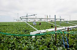
In studies at Urbana, Illinois, ARS scientists (left to right) Carl Bernacchi, Don Ort, and Lisa Ainsworth work in a facility where photosynthesis efficiency and yield can be measured in response to a simulated variable. Improving photosynthesis could lead to increased food production from soybeans, shown here. Photo courtesy of Institute for Genomic Biology/University of Illinois.

Scientists now have a way to more accurately compare how efficiently plants and photovoltaic, or solar, cells convert sunlight into energy, thanks to findings by a research consortium that included a U.S. Department of Agriculture (USDA) scientist.

The study, published in Science, could help researchers improve plant photosynthesis, a critical first link in the global supply chain for food, feed, fiber and bioenergy production.

Comparing plant and photovoltaic systems is a challenge. Although both processes harvest energy from sunlight, they use that energy in different ways. Plants convert the sun's energy into chemical energy, whereas solar cells produce electricity. The scientists, including Agricultural Research Service (ARS) research leader Donald Ort in the agency's Global Change and Photosynthesis Research Unit in Urbana, Ill., identified specific designs that hold excellent promise for improving efficiency.

ARS is the USDA's chief intramural scientific research agency.

The first step was to facilitate a direct comparison of the two systems. The researchers set a uniform basis for the comparison and examined the major factors that define the efficiencies of both processes, first considering current technology, then looking forward to possible strategies for improvements.

In all cases, the research team considered the efficiency of harvesting the entire solar spectrum as a basis for comparison. Additionally, the researchers compared plants to solar cell arrays that also store energy in chemical bonds. Calculations were applied to a solar cell array that was coupled to an electrolyzer that used electricity from the array to split water into hydrogen and oxygen. The free energy needed to split water is essentially the same as that needed for photosynthesis or a solar cell, so the comparison provided a level playing field.

Using this type of calculation, the annual averaged efficiency of solar-cell-driven electrolysis is about 10 percent. Solar energy conversion efficiencies for crop plants are about 1 percent, which illustrates the significant potential to improve the efficiency of the natural system, according to Ort. While, in the context of the team's efficiency analysis, solar cells have a clear advantage compared to photosynthesis, there is a need to apply both in the service of sustainable energy conversion for the future. This energy-efficiency analysis between plant photosynthesis and solar cells will lay the groundwork for improving the efficiency of plant photosynthesis in agriculture for improved yield.

Source: Agricultural Research Service

Nano-engineered carbons promise better gas storage materials for advanced transportation

Engineerblogger
Jan 17, 2012


Tunable sub-nm and supra-nm pores in KOH-activated carbon

Activated carbons provide large surface areas (as high as 3000 m2/g) generated by a maze of nanoscale pores for high-performance adsorption. Applications include the storage of hydrogen and natural gas for advanced transportation (pressure-controlled adsorption/desorption of gas at supercritical temperature). Here, two distinct types of pores have attracted the interest of researchers: sub-nm (<1 nm) pores host deep potential wells – surface sites with high binding energies – which adsorb gas molecules as a high-density fluid; supra-nm (>1 nm) pores host lower binding energies, but offer space for multilayer adsorption. In addition, sub-nm pores favour high volumetric storage capacity; supra-nm pores favour high gravimetric storage capacity. Experts are looking for ways to optimize gas storage capacities by controlling the number of pores in each of the two classes.

In a recent study, published in the journal Nanotechnology, scientists at the University of Missouri, US, have demonstrated that such control is possible. Carbons chemically activated with potassium hydroxide (carbon oxidation; intercalation of metallic potassium into carbon lattice) gave bimodal pore-size distributions with a large, approximately constant number of sub-nm pores and variable number of supra-nm pores (1–5 nm, peaked around 1.5 nm). The control variables were the KOH:C mass ratio and activation temperature.

Tunable pore space

The team showed that supra-nm pores are absent when the KOH:C ratio and activation temperature are low, and increase rapidly in number with increasing KOH:C ratio and activation temperature. By appropriate choice of the variables, the volume in supra-nm pores can be varied anywhere from 0 to 1.0 cm3/g, while the volume in sub-nm remains approximately 0.6 cm3/g.

This tunable pore space will allow researchers to selectively optimize carbons for high volumetric or high gravimetric storage capacity, depending on the requirements in different vehicles for on-board storage of hydrogen and natural gas.

High volumetric capacity is important for designs where space is limited (passenger vehicles - light duty vehicles) and a high gravimetric capacity is key when vehicle weight must be kept to a minimum.

The research was conducted by members of the Alliance for Collaborative Research in Alternative Fuel Technology (ALL-CRAFT), a partnership of the University of Missouri and several other institutions, funded by the National Science Foundation, US Department of Energy, US Department of Defense, California Energy Commission, and Southern California Gas Company, to develop novel storage materials for natural gas and hydrogen for advanced next-generation clean vehicles.

 Source: IOP Publishing

Additional Information:

Monday, January 16, 2012

Magnetic Memory Miniaturized to Just 12 Atoms

Technology Review
Jan 16, 2012


This scanning tunneling microscope image shows a group of 12 iron atoms, the smallest magnetic memory bit ever made. Credit: IBM


The smallest magnetic-memory bit ever made—an aggregation of just 12 iron atoms created by researchers at IBM—shows the ultimate limits of future data-storage systems.

The magnetic memory elements don't work in the same way that today's hard drives work, and, in theory, they can be much smaller without becoming unstable. Data-storage arrays made from these atomic bits would be about 100 times denser than anything that can be built today. But the 12 atoms making up each bit must be painstakingly assembled using an expensive and complex microscope, and the bits can hold data for only a few hours and at low temperatures approaching absolute zero, so the miniscule memory elements won't be found in consumer devices anytime soon.

As the semiconductor industry bumps up against the limits of scaling by making memory and computation devices ever smaller, the IBM Almaden research group, led by Andreas Heinrich, is working from the other end, building computing elements atom-by-atom in the lab.

The necessary technology for large-scale manufacturing at the single-atom scale doesn't exist yet. Today, says Heinrich, the question is, "What is it you would want to build on the scale of atoms for data storage and computation, in the distant future?"

As engineers miniaturize conventional devices, they're finding that quantum physics, which never had to be accounted for in the past, makes devices less stable. As conventional magnetic memory bits are miniaturized, for example, each bit's magnetic field begins to affect its neighbors', weakening each bit's ability to hold on to a 1 or a 0.

The IBM researchers found that it was possible to sidestep this problem by using groups of atoms that display a different kind of magnetism. The key, says Heinrich, is the magnetic spin of each individual atom.
To read more click here...

Friday, January 13, 2012

"Open-source" robotic surgery platform going to top medical research labs

Engineerblogger
Jan 12, 2012


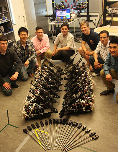
Team members posed with components of the Raven II surgical robotic systems developed in the Bionics Lab at the Baskin School of Engineering. From left to right: Zachary Wells (bioengineering undergraduate), Calvin Yoo (bioengineering undergraduate), lab director Jacob Rosen (associate professor of computer engineering), Ji Ma (postdoctoral researcher), Joshua Schloemer (economics undergraduate), Farhad Ighani (computer engineering undergraduate), and Kyle Fujisawa (computer engineering undergraduate). (Photo by Carolyn Lagattuta)


Robotics experts at UC Santa Cruz and the University of Washington (UW) have completed a set of seven advanced robotic surgery systems for use by major medical research laboratories throughout the United States. After a round of final tests, five of the systems will be shipped to medical robotics researchers at Harvard University, Johns Hopkins University, University of Nebraska, UC Berkeley, and UCLA, while the other two systems will remain at UC Santa Cruz and UW.

"We decided to follow an open-source model, because if all of these labs have a common research platform for doing robotic surgery, the whole field will be able to advance more quickly," said Jacob Rosen, associate professor of computer engineering in the Baskin School of Engineering at UCSC and principal investigator on the project.

Rosen and Blake Hannaford, director of the UW Biorobotics Laboratory, lead the research groups that developed the Raven II robotic surgery system and its predecessor, Raven I. A grant from the National Science Foundation funded their work to create seven identical Raven II systems. Hannaford said the systems will be shipped out from UW by the end of January. After they are delivered and installed, all seven systems will be networked together over the Internet for collaborative experiments.

Robotic surgery has the potential to enable new surgical procedures that are less invasive than existing techniques. For some procedures, such as prostate surgery, the use of surgical robots is already standard practice. In addition, telesurgery, in which the surgeon operates a robotic system from a remote location, offers the potential to provide better access to expert care in remote areas and the developing world. Having a network of laboratories working on a common platform will make it easier for researchers to share software, replicate experiments, and collaborate in other ways.

Even though it meant giving competing laboratories the tools that had taken them years to develop, Rosen and Hannaford decided to share the Raven II because it seemed like the best way to move the field forward. "These are the leading labs in the nation in the field of surgical robotics, and with everyone working on the same platform we can more easily share new developments and innovations," Hannaford said.

According to Rosen, most research on surgical robotics in the United States has focused on developing new software for various commercially available robotic systems. "Academic researchers have had limited access to these proprietary systems. We are changing that by providing high-quality hardware developed within academia. Each lab will start with an identical, fully-operational system, but they can change the hardware and software and share new developments and algorithms, while retaining intellectual property rights for their own innovations," Rosen said.

The Raven II includes a surgical robot with two robotic arms, a camera for viewing the operational field, and a surgeon-interface system for remote operation of the robot. The system is powerful and precise enough to support research on advanced robotic surgery techniques, including online telesurgery.

In addition to Rosen and Hannaford, UCSC postdoctoral researchers Daniel Glozman and Ji Ma, along with a group of dedicated undergraduate students working in Rosen's Bionics Lab, played a key role in developing the Raven II. Rosen and Glozman have also developed a Raven IV surgical robotics system, which includes four robotic arms and two cameras. The system enables collaboration between two surgeons working from separate locations and connected over the Internet.

Source: University of California - Santa Cruz

Thursday, January 12, 2012

Broad scientific approach to studying rare earth materials needed to ensure continued deployment of clean energy technologies

Lawrence Berkeley National Laboratory
Jan 11, 2012 


The top matrix shows the supply risk and importance to clean energy of certain elements in the short term (present-2015). The bottom matrix shows the medium term (2015-2025). (Source: DOE)

A few short decades ago, few could have imagined that the world would be seriously concerned over something called dysprosium. Also known as number 66 on the periodic table, dysprosium was once just another element for chemistry students to memorize but is now one of the most sought-after and critically needed materials on the planet.

Belonging to a family of elements known as lanthanides—also called rare earths—dysprosium and other rare earths are used in almost every high-tech gadget and clean energy technology invented in the last 30 years, from smart phones to wind turbines to hybrid cars. Although the United States was self-sufficient in rare earths or obtained them on the free market until the early 2000s, the vast majority are now mined in China and the supply has been subject to fluctuations. The Department of Energy’s (DOE) Lawrence Berkeley National Laboratory (Berkeley Lab) aims to change the status quo by reviving the study of these critical materials to better understand how to extract them, use them more efficiently, reuse and recycle them and find substitutes for them.

In its 2011 Critical Material Strategy released last month, the DOE said that “supply challenges for five rare earth metals (dysprosium, neodymium, terbium, europium and yttrium) may affect clean energy technology deployment in the years ahead.” It also recommended enhanced training of scientists and engineers to “address vulnerabilities and realize opportunities related to critical materials.”

“If we are going to achieve what we need to do in terms of managing climate change, we absolutely have to fix the materials problem—it’s the linchpin for clean energy technologies,” said Frances Houle, a Berkeley Lab scientist who is Director of Strategic Initiatives in the Chemical Sciences Division. “Because Berkeley Lab is such a broad institution, many of the pieces required are already here. We have the chemistry, the earth science, the materials science, the theory. Not very many institutions can say that.”

Like coal and gold, the rare earths are mined out of the ground. However, in any given ore, they are mixed together with other rare earths. So although they are not actually rare, they are difficult to mine. “They’re in low concentration, and it’s very hard to mine them and separate them out, so it’s challenging and extremely energy-intensive to produce rare earth materials ready for industrial manufacturers; it requires a lot of electricity, water and chemicals,” said Berkeley Lab Senior Scientist David Shuh. “This area of study has been ignored over the last two decades, largely due to insufficient research and development support.”
To read more click here...

Metal oxide simulations could help green technology

Engineerblogger
Jan 12, 2012


Computer simulations show that metal oxides in water go through many short-lived shapes and structures. (William Casey/UC Davis graphic)


University of California, Davis, researchers have proposed a radical new way of thinking about the chemical reactions between water and metal oxides, the most common minerals on Earth. Their work appears in the current issue of the journal Nature Materials.

The new paradigm could lead to a better understanding of corrosion and how toxic minerals leach from rocks and soil. It could also help in the development of “green” technology: new types of batteries, for example, or catalysts for splitting water to produce hydrogen fuel.

“This is a global change in how people should view these processes,” said William Casey, UC Davis professor of chemistry and co-author of the study with James Rustad, a former geology professor at UC Davis who now works as a scientist at Corning Inc. in New York.

Previously, when studying the interactions of water with clusters of metal oxides, researchers tried to pick and study individual atoms to assess their reactivity. But “none of it really made sense,” Rustad said.

Using computer simulations developed by Rustad, and comparing the resulting animations with lab experiments by Casey, the two found that the behavior of an atom on the surface of the cluster can be affected by an atom some distance away.

Instead of moving through a sequence of transitional forms, as had been assumed, metal oxides interacting with water fall into a variety of “metastable states” — short-lived intermediates, the researchers found.

For example, in one of Rustad’s animations, a water molecule approaches an oxygen atom on the surface of a cluster. The oxygen suddenly pulls away from another atom binding it into the middle of the cluster and leaps to the water molecule. Then the structure collapses back into place, ejecting a spare oxygen atom and incorporating the new one.

The U.S. Department of Energy and the National Science Foundation sponsored the research.

Source: University of California, Davis

Wednesday, January 11, 2012

Stretching Exercises: Using Digital Images to Understand Bridge Failures

Engineerblogger
Jan 11, 2012


Photogrammetry at work: New video shows how NIST and the FHWA used random patterns of speckles painted on metal to better understand how stress and strain could lead to catastrophic failure.


With a random-looking spatter of paint specks, a pair of cameras and a whole lot of computer processing, engineer Mark Iadicola of the National Institute of Standards and Technology (NIST) has been helping the Federal Highway Administration (FHWA), in cooperation with the American Association of State Highway and Transportation Officials (AASHTO), to assure the safety of hundreds of truss bridges across the United States. Iadicola has been testing the use of a thoroughly modern version of an old technique—photographic measurement or “photogrammetry”—to watch the failure of a key bridge component in exquisite detail.

The impetus for the FHWA project was the disastrous collapse of the Interstate 35-W bridge in Minneapolis, Minnesota. On Aug. 1, 2007, in the middle of the evening rush hour, a thousand feet of the bridge’s main deck truss collapsed, part of it falling 108 feet into the Mississippi River. Thirteen people died. One hundred and forty five were injured.

According to FHWA engineer Justin Ocel, an investigation by the National Transportation Safety Board (NTSB), assisted by FHWA, determined that the immediate culprit was a failed gusset plate, a flat heavy piece of steel bolted in pairs to join the ends of the steel members that make up the bridge truss. As a result of a design error decades before, the gusset plates in the bridge were about half as thick as they should have been.

Although that design flaw was clearly a major factor in the disaster, Ocel says, the collapse highlighted the fact that gusset plates were not generally considered by engineers during periodic reviews of bridge capacity, a process called load rating. It was assumed that gusset plates were properly sized to be stronger than the members they connect. “One of the recommendations from the NTSB was that we include gusset plates in load ratings, and until that point it hadn't been done,” Ocel explains. “To assist the states with this process we developed a guidance document on how to load rate gusset plates.”

In developing the guidance, Ocel says, FHWA used the best available data on the failure modes of gusset plates in major bridges—but there wasn’t much. So at the FHWA's Turner-Fairbank Highway Research Center in Virginia they began building full-scale models of bridge gusset plate joints and pulling them apart with a huge hydraulic test machine.

NIST’s Iadicola is there to watch what happens as the plate stretches and fails. He covers the plate with an irregular pattern of paint speckles and then trains a pair of carefully calibrated, high-definition digital cameras on it. The cameras repeatedly image the plate, send the pictures to a computer that uses custom software to compare each image to the previous one, and calculate which of the paint spots have moved, in what direction and by how much. Using two cameras allows the computer to “see” the plate in three dimensions, so it can tell if points on the surface move in or out as well as up, down or sideways.

“The NIST digital image correlation method is a good complement to the FHWA measurement methods,” Iadicola explains. “Their techniques—strain gages and photoelasticity—are very good for the normal range of stress in which the plate will stretch and spring right back to its original shape. Our method can tell you a little about that, but it really shines in showing you what happens past that point, when the plate starts permanently deforming and finally rips apart. The failure modes.”

After more than a year of experiments, Ocel says, the FHWA has learned a lot about how to predict what loads will cause a gusset plate to fail. Currently, FHWA is working with AASHTO to translate those findings into language that can be adopted into the AASHTO Bridge Design Specification and Manual for Bridge Evaluation, two documents used throughout the country for designing and load rating bridges.

The FHWA project is just one of a range of applications for digital image correlation being studied at NIST, Iadicola says. “We’ve been using it in looking at sheet metal forming—you have very high strains during the forming process—and we’ve used it at very small scales, looking at targets with an optical microscope.”

Source: The National Institute of Standards and Technology (NIST)

Tuesday, January 10, 2012

Can We Build Tomorrow's Breakthroughs?

Technology Review
Jan 10, 2012


Powering up: GE’s new facility will make an innovative type of battery for data centers and backup power. Credit: Ian Allen


In a hangarlike building where General Electric once assembled steam turbines, a $100 million battery manufacturing facility is being constructed to make products using a chemistry never before commercialized on such a large scale. The sodium–metal halide batteries it will produce have been tested and optimized over the last few years by a team of materials scientists and engineers at GE's sprawling research center just a few miles away. Now some of the same researchers are responsible for reproducing those results in a production facility large enough to hold three and a half football fields.

The engineers have moved from the bucolic research center, which sits on a hill overlooking the Mohawk River, down to the manufacturing site, which abuts the river at the edge of Schenectady, New York, a working-class town known in its heyday as Electric City. There, they supervise the installation and testing of robotics, high-temperature kilns, and analytic equipment that will monitor the production process. The new batteries use an advanced ceramic as an electrolyte inside a sealed metal case containing nickel chloride and sodium; the technology promises to store three times as much energy as the lead-acid batteries used in data centers, in heavy-duty electric vehicles, and for backup power. But almost anything can go wrong. If, say, the particles that make up the ceramic are uneven in size or haven't been properly dried, battery performance could fall short. That means the conditions in the huge factory must be tightly controlled, and multi-ton devices must be able to match the exactness of lab equipment. "It's not for the weak of heart," says Michael ­Idelchik, GE's vice president of advanced technologies.

The GE plant is one of a number of facilities around the country producing new technologies for rapidly growing markets in advanced batteries, electric vehicles, and solar power—but those efforts cannot counter the reality that the U.S. manufacturing sector is in trouble. After decades of outsourcing production in an effort to lower costs, many large companies have lost the expertise for the complex engineering and design tasks necessary to scale up and produce today's most innovative new technologies, not to mention the appetite for the risks involved.

If you believe Thomas Friedman's assertion that "the world is flat," and that moving manufacturing to places where production is cheap makes companies more competitive, such a shift might not matter beyond its implications for the U.S. economy and its workers. But the United States remains the world's most prolific source of new technologies, particularly materials-based ones, and evidence is growing that its diminished manufacturing capabilities could severely cripple global innovation. There are ample reasons to believe that the model of the U.S. computer industry—which has successfully outsourced much of its production in the last few decades and made design, not manufacturing, its priority—will not work effectively for companies trying to commercialize innovations in energy, advanced materials, and other emerging sectors.

Academic researchers have begun documenting the complex connections between innovation and manufacturing with an eye to clarifying how the loss of U.S. manufacturing could affect the emergence of new technologies. Willy Shih, a professor of management at Harvard Business School, has created a list of basic technologies in which the United States has squandered its lead in manufacturing in recent years. They include crystalline silicon wafers, LCDs, power semiconductors for solar cells, and many types of advanced batteries. And he has detailed how losing the "industrial commons"—the research know-how, engineering skills, and manufacturing expertise needed to make a specific technology—can often mean losing the knowledge and incentives to create advances in related technologies. For example, as silicon semiconductor production and associated supply chains have shifted to Asia, the development of new silicon-based solar cells has been hampered in the United States.

It turns out it's not necessarily true that innovative technologies will simply be manufactured elsewhere if it doesn't happen in the United States. According to research by Erica Fuchs, an assistant professor at Carnegie Mellon University, the development of integrated photonics, in which lasers and modulators are squeezed onto a single chip, has been largely abandoned by optoelectronic manufacturers as they have moved production away from the United States. Many telecom firms were forced to seek lower-cost production in East Asia after the industry's collapse in the early 2000s, and differences in manufacturing practices meant that producing integrated photonic chips was not economically viable in those countries. Thus a technology that once appeared to be just a few years away from revolutionizing computers and even biosensors was forsaken. Economists might argue that we don't care where something is produced, says Fuchs, but location can profoundly affect "the products that you choose to make and the technology trajectory itself."

For many people in industry, the connections between innovation and manufacturing are a given—and a reason to worry. "We have learned that without a foothold in manufacturing, the ability to innovate is significantly compromised," says GE's Idelchik. The problem with outsourcing production is not just that you eventually lose your engineering expertise but that "businesses become dependent on someone else's innovation for next-generation products." One repercussion, he says, is that researchers and engineers lose their understanding of the manufacturing process and what it can do: "You can design anything you want, but if no one can manufacture it, who cares?"

After decades as the world's largest manufacturer, the United States now makes, according to some recent estimates, 19.4 percent of the world's manufactured goods—second to China, which makes 19.8 percent. Even in high-tech products, the United States now imports more than it makes. Those statistics have implications for employment, national competitiveness, and even the politics and social structure of the country. But equally worrisome, especially over the long term, is what the declining ability of the United States to make stuff implies for the next generation of technology. Can the United States regain its ability to take on high-risk manufacturing? To ask the same question in a different way, are many of today's most promising innovations in danger of suffering the same fate as integrated photonic chips?
To read more click here...

Monday, January 9, 2012

Layer by Layer: 3D printing makes existing products more efficiently and creates complex components

Engineerblogger
Jan 9, 2012

Buildup: GE made the aircraft engine ­component on the left by using a laser to melt metal in precise places, beginning with the single layer seen on the right. Credit: Bob O’Connor

The parts in jet engines have to withstand staggering forces and temperatures, and they have to be as light as possible to save on fuel. That means it's complex and costly to make them: technicians at General Electric weld together as many as 20 separate pieces of metal to achieve a shape that efficiently mixes fuel and air in a fuel injector. But for a new engine coming out next year, GE thinks it has a better way to make fuel injectors: by printing them.

To do it, a laser traces out the shape of the injector's cross-section on a bed of cobalt-chrome powder, fusing the powder into solid form to build up the injector one ultrathin layer at a time. This promises to be less expensive than traditional manufacturing methods, and it should lead to a lighter part—which is to say a better one. The first parts will go into jet engines, says Prabhjot Singh, who runs a lab at GE that focuses on improving and applying this and similar 3-D printing processes. But, he adds, "there's not a day we don't hear from one of the other divisions at GE interested in using this technology."

These innovations are at the forefront of a radical change in manufacturing technology that is especially appealing in advanced applications like aerospace and cars. The 3-D printing techniques won't just make it more efficient to produce existing parts. They will also make it possible to produce things that weren't even conceivable before—like parts with complex, scooped-out shapes that minimize weight without sacrificing strength. Unlike machining processes, which can leave up to 90 percent of the material on the floor, 3-D printing leaves virtually no waste—a huge consideration with expensive metals such as titanium. The technology could also reduce the need to store parts in inventory, because it's just as easy to print another part—or an improved version of it—10 years after the first one was made. An automobile manufacturer receiving reports of a failure in a seat belt mechanism could have a reconfigured version on its way to dealers within days.

Additive manufacturing, as 3-D printing is also known, emerged in the mid-1980s after Charles Hull invented what he called stereo­lithography, in which the top layer of a pool of resin is hardened by an ultraviolet laser. Various methods of 3-D printing have become popular with engineers who want to create prototypes of new designs or make a few highly customized parts: they can make a 3-D blueprint of a part in a computer-assisted design program and then get a printer to spit it out hours later. This process avoids the up-front costs, long lead times, and design constraints of conventional high-volume manufacturing techniques like injection molding, casting, and stamping. But the technology has been adapted to only a limited set of materials, and there have been questions about quality control. Building parts this way has also been slow—it can take a day or more to do what traditional manufacturing can accomplish in minutes or hours. For these reasons, 3-D printing hasn't been used for very large runs of production parts.

But now the technology is advancing far enough for production runs in niche markets such as medical devices. And it's poised to break into several larger applications over the next several years. "We've come to the point when enough critical advances are happening to make the technology truly useful in manufacturing end-use parts," says Tim Gornet, who runs the Rapid Prototyping Center at the University of Louisville.


Pressing print: This photo shows an array of metal jet-engine components printed at GE. Credit: Bob O’Connor

MAKING INROADS

Several techniques can be used to "print" a solid object layer by layer. In sintering, a thin layer of powdered metal or thermoplastic is exposed to a laser or electron beam that fuses the material into a solid in designated areas; then a new coating of powder is laid on top and the process repeated. Parts can also be built up with heated plastic or metal extruded or squirted through a nozzle that moves to create the shape of one layer, after which another layer is deposited directly on top, and so forth. In another 3-D printing method, glue is used to bind powders.

Aerospace companies are at the forefront of adopting the technology, because airplanes often need parts with complex geometries to meet tricky airflow and cooling requirements in jammed compartments. About 20,000 parts made by laser sintering are already flying in military and commercial aircraft made by Boeing, including 32 different components for its 787 Dreamliner planes, according to Terry Wohlers, a manufacturing consultant who specializes in additive processes. These aren't items that have to be mass-produced; Boeing might make a few hundred of them all year. They're also not critical to flight; among them are elaborately shaped air ducts needed for cooling, which previously had to be manufactured in multiple pieces. "Now we can optimize the design of these parts for weight, and we save material and labor," says Mike Vander Wel, director of Boeing's manufacturing technology strategy group. "In theory, this is the ultimate manufacturing method for us." Though the speed limitations of 3-D printing might keep it from ever producing the majority of Boeing's parts, Vander Wel says, the approach is likely to be used in a growing proportion of them.

Boeing's main rival, the European Aeronautic Defense and Space Company (EADS), is using the technology to make titanium parts in satellites and hopes to use it for parts it makes in higher volume for Airbus planes. "We don't yet know what the extent of our use of additive-layer manufacturing there will be yet, but we don't see any show stoppers," says Jon Meyer, who heads research on 3-D printing at EADS's Innovation Works division in England.


Smaller scale: Seen here is a microprinter that GE uses to test new ways of building things out of ceramic materials. Researchers are using the machine to print the transducers used as probes in ultrasound machines; they believe it might save time and money while improving design. Credit: Bob O’Connor

GE's jet engine division may be closer than anyone else to bringing 3-D-printed parts into large-scale commercial production. In addition to the fuel injector, GE is also laser-sintering titanium into complex shapes for four-foot-long strips bonded onto the leading edge of fan blades. These strips deflect debris and create more efficient airflow. Until now, each one has required tens of hours of forging and machining, during which 50 percent of the titanium was lost. By switching to 3-D printing, the company will save about $25,000 in labor and material in each engine, estimates Todd Rockstroh, the GE consulting engineer who heads the effort. The blade edge and the fuel injector will start appearing in engines as early as 2013, and they will be integrated into full-scale production runs in the thousands by about 2016.

Meanwhile, says Rockstroh, the company hopes to gain design flexibility by using 3-D printing for more parts. When it recently discovered that a stem in the fuel injector was subjected to excessive levels of heat stress, a redesigned version came out of the printer within a week. "Before, we would have had to redesign 20 different parts, with all the associated tooling," says Rockstroh. "It might not have even been possible." And using 3-D printing to corrugate the insides of some parts can reduce their weight by up to 70 percent, which can save an airline millions of gallons of fuel every year. That prospect has GE looking for ways to print everything from gearbox housings to control mechanisms. "We're going on a major weight-reduction scavenger hunt next year," Rockstroh says.

Automobiles could similarly benefit from lighter parts, and the University of Louisville's Gornet notes that printing processes could cut the weight of valves, pistons, and fuel injectors by at least half. Some manufacturers of ultraluxury and high-performance cars, including Bentley and BMW, are already using 3D printing for parts with production runs in the hundreds.


Polished: A transducer made in GE’s microprinter (top) and the same transducer after being refined and finished in other machines (bottom). Credit: Bob O’Connor

CHALLENGES TO OVERCOME

If it weren't for the limitations of the technology, 3-D printing would already be much more broadly used. "Speeds are atrociously slow right now," says GE's Singh. Todd Grimm, who heads an additive-­manufacturing consultancy in Edgewood, Kentucky, estimates that the time it takes to produce a part will have to improve as much as a hundredfold if 3-D printing is to compete directly with conventional manufacturing techniques in most applications. That won't happen in the next few years.

Another problem: for now, only a handful of plastic and metal compounds can be used in 3-D printing. In laser sintering, for example, the material must be able to form a powder that will melt neatly when it is hit with a laser, and then solidify quickly. The compounds that meet the necessary criteria can cost 50 to 100 times as much by weight as the raw materials used in conventional manufacturing processes, partly because they're in such low demand that they're available only from small specialty suppliers.

As demand increases with new applications, however, supplier competition should pull prices down dramatically. And the list of available materials is slowly expanding. GE is trying to use ceramics, which would open up new possibilities in engines and medical devices, among other areas.

Simple experience, too, will do much to improve the technology. So far, manufacturers don't have enough data to predict exactly how a part will turn out and how it will hold up, or how production variables—including temperature, choice of material, part shape, and cooling time—affect the results. That can be frustrating, says Singh: "3-D printing often ends up being a black art. A part is made out of thousands of layers, and each layer is a potential failure mode. We still don't understand why a part comes out slightly differently on one machine than it does on another, or even on the same machine on a different day." For example, the layering process tends to build up interlayer stresses in unpredictable ways, so that some parts end up distorted. Porosity can vary within parts as well, leading to concerns about fatigue or brittleness. That could be a big problem in aircraft engines or wing struts. "We know how to make the metals strong enough," says Boeing's Vander Wel. "But we worry about the unpredictability. Can we repeat a result to get 100 parts that are exactly the same? We're not sure yet."

Even with these challenges, time is on the side of 3-D printing, says Vander Wel, and not just because the processes are improving. Engineers are understandably reluctant to embrace a new technology for critical parts when their deadlines and reputations, not to mention the lives of people in airplanes, are at stake. "But younger designers are adapting more quickly," he says. "They're not so quick to say, 'It can't be built this way.'"

Source: Technology Review